Integrated circuit having structural support for a flip-chip interconnect pad and method therefor

a technology of flip-chip interconnect pads and integrated circuits, which is applied in the direction of semiconductor devices, semiconductor/solid-state device details, electrical apparatuses, etc., can solve the problems of increased stress on the bond pad structure, low dielectric constant (low-k) dielectrics susceptible to mechanical damage, and bond pad structures fabricated with copper interconnect metallization and low-k dielectrics are susceptible to mechanical damag

Active Publication Date: 2007-07-24
VLSI TECH LLC
View PDF13 Cites 11 Cited by
  • Summary
  • Abstract
  • Description
  • Claims
  • Application Information

AI Technical Summary

Problems solved by technology

A smaller bond pad region results in increased stress to the bond pad structure when physical connection is made to the semiconductor die.
Bond pad structures fabricated with copper interconnect metallization and low dielectric constant (low-k) dielectrics are susceptible to mechanical damage during the bonding process.
As a result, dielectric cracking and delamination of layers under the flip chip bond pads result from package-to-die Coefficient of Thermal Expansion (CTE) mismatch stresses.
This via arrangement requires that majority portions of the underlying metal layers and the bonding pad are all electrically connected together and thus are not functionally independent of each other.

Method used


Image

  • Integrated circuit having structural support for a flip-chip interconnect pad and method therefor
  • Integrated circuit having structural support for a flip-chip interconnect pad and method therefor
  • Integrated circuit having structural support for a flip-chip interconnect pad and method therefor

Examples


Embodiment Construction

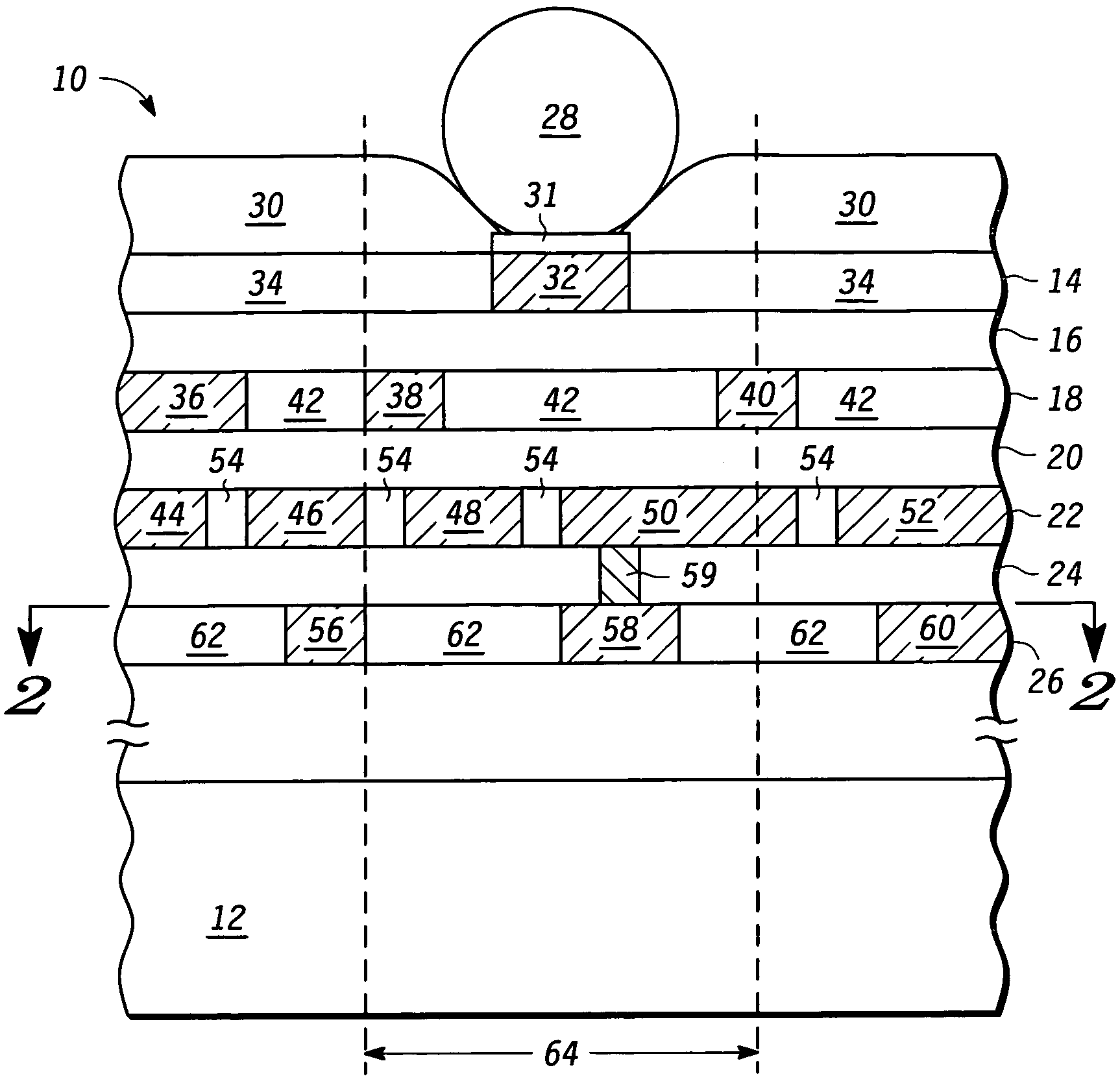
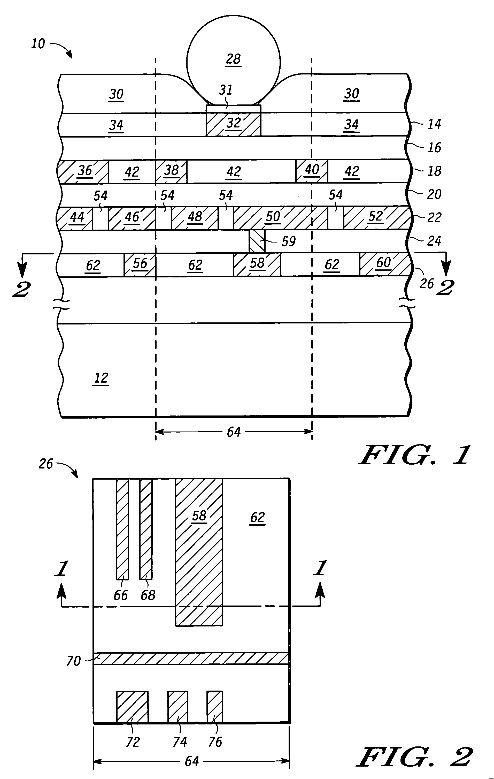
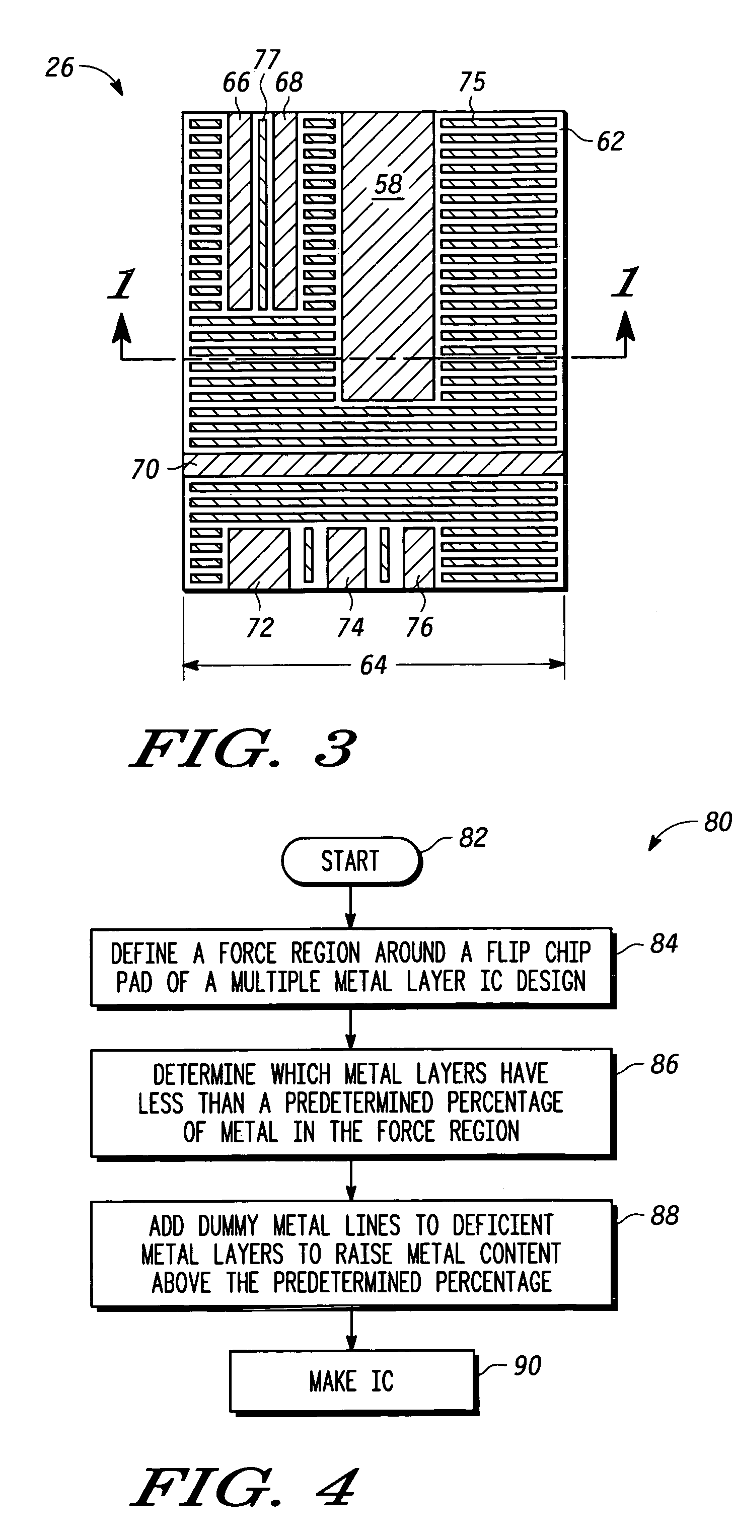
[0013]Generally there is herein provided a method and apparatus for providing structural support for interconnect pad locations in an integrated circuit (IC) by using novel layout techniques in the metallization and dielectric stack underlying the pad. As used herein, an interconnect pad, formed of metal, is placed at the surface of an integrated circuit where an electrical connection is made from the pad to one or more underlying interconnect layers. In a typical IC design, multiple interconnect layers separated by interlevel dielectrics are formed in a stack to provide the required interconnections between devices in the semiconductor substrate. Examples of an interconnect pad include, but are not limited to, a wire bond pad, a probe pad, a flip-chip bump pad, a test point or other packaging or test pad structures that may require underlying structural support. The interconnect pad region, located physically underneath the interconnect pad, defines the region in which the layout t...


PUM


Abstract

A technique for alleviating the problems of defects caused by stress applied to bond pads (32) includes, prior to actually making an integrated circuit (10), adding dummy metal lines (74, 76) to interconnect layers (18, 22, 26) to increase the metal density of the interconnect layers. These problems are more likely when the interlayer dielectrics (16, 20, 24) between the interconnect layers are of a low-k material. A critical area or force area (64) around and under each bond pad defines an area in which a defect may occur due to a contact made to that bond pad. Any interconnect layer in such a critical area that has a metal density below a certain percentage can be the cause of a defect in the interconnect layers. Any interconnect layer that has a metal density below that percentage in the critical area has dummy metal lines added to it.

Description

CROSS REFERENCE TO RELATED APPLICATION[0001]This application is related to copending U.S. patent application Ser. No. 11 / 033,008 entitled “Method and Apparatus for Providing Structural Support For Interconnect Pad While Allowing Signal Conductance” filed simultaneously herewith by Kevin Hess et al. and assigned to the assignee hereof.FIELD OF THE INVENTION[0002]This disclosure relates to packaged semiconductors and more particularly to interconnect pads of integrated circuits for making electrical connection to underlying conductive layers.RELATED ART[0003]The use of conductive balls, such as solder balls, to make electrical connection to a bond pad is a known method to make electrical connection to electrical circuitry of a semiconductor die. Conductive ball packaging is commonly known in the industry as flip chip interconnect. As geometries in semiconductors continue to shrink in size due to improvements in the technology for making semiconductors, the sizes of bond pad regions ha...

Claims


Application Information

Patent Timeline
Patent Type & Authority Patents(United States)
IPC IPC(8): H01L21/4763
CPCH01L23/522H01L24/02H01L24/13H01L24/10H01L2224/0401H01L2224/13099H01L2224/16H01L2924/01013H01L2924/01014H01L2924/01029H01L2924/014H01L2924/14H01L2924/01019H01L2924/01033H01L2924/00H01L2224/13H01L24/05
Inventor POZDER, SCOTT K.HESS, KEVIN J.LEUNG, PAK K.TRAVIS, EDWARD O.WILKERSON, BRETT P.WONTOR, DAVID G.ZHAO, JIE-HUA
Owner VLSI TECH LLC
Why Eureka
Try Eureka