Integrated carbon nanotube sensors

a carbon nanotube and sensor technology, applied in nanoinformatics, instruments, transistors, etc., can solve the problems of affecting the operation of the chip, affecting the performance of the critical circuit, and unable to specifically pinpoint, and unable to achieve specific pinpointing

Inactive Publication Date: 2007-07-24
INT BUSINESS MASCH CORP
View PDF11 Cites 24 Cited by
  • Summary
  • Abstract
  • Description
  • Claims
  • Application Information

AI Technical Summary

Benefits of technology

[0010]According to the embodiments of the invention, the CNT FET has enhanced resolution qualities, has the capability of being operable at both the wafer level or on packaged parts, is configured small enough such that it does not occupy significant chip area, and is configured such that it does not negatively impact circuit and / or device performance. The embodiments of the invention may be incorporated in microprocessors, application-specific integrated circuits, SRAM configurations, arrays of memory cells, macros, cores, and digital or analog circuit elements that have a known physical design for detection of specific defects or specific characterization of the circuit element. For example, the embodiments of the invention may be used for power use analysis, thermal characterization, IDD, critical path analysis, as well as other on-chip testing and diagnostic parameters affecting device performance.

Problems solved by technology

Unfortunately, electrical readout circuitry generally occupies valuable chip area, induces performance degradation or load to critical circuits on the chip, and cannot specifically pinpoint the location of problems.
Furthermore, remote sensing using physical sensors from the front side of chips is typically blocked by metal wiring and surface interconnects or input / output (I / O) devices.
From the back side, signals tend to be severely attenuated by the silicon substrate and blocked by metal wiring as from the front side.
Moreover, remote sensors are also generally lacking with regard to spatial resolution, where the best case has shown to be approximately on the order of one micron, which is already ten times greater than the minimum integrated circuit features.

Method used


Image

  • Integrated carbon nanotube sensors
  • Integrated carbon nanotube sensors
  • Integrated carbon nanotube sensors

Examples


Embodiment Construction

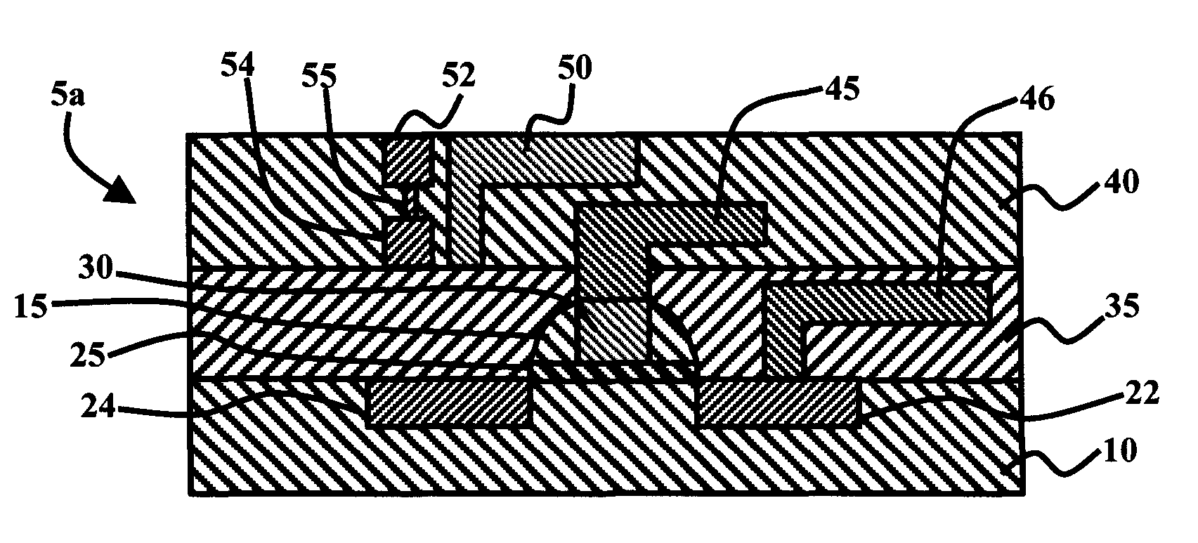
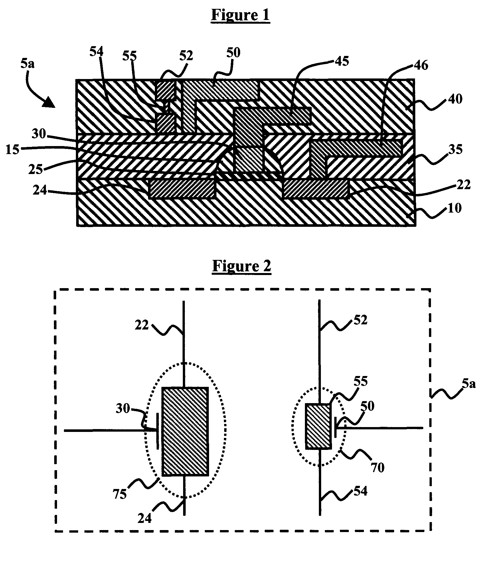
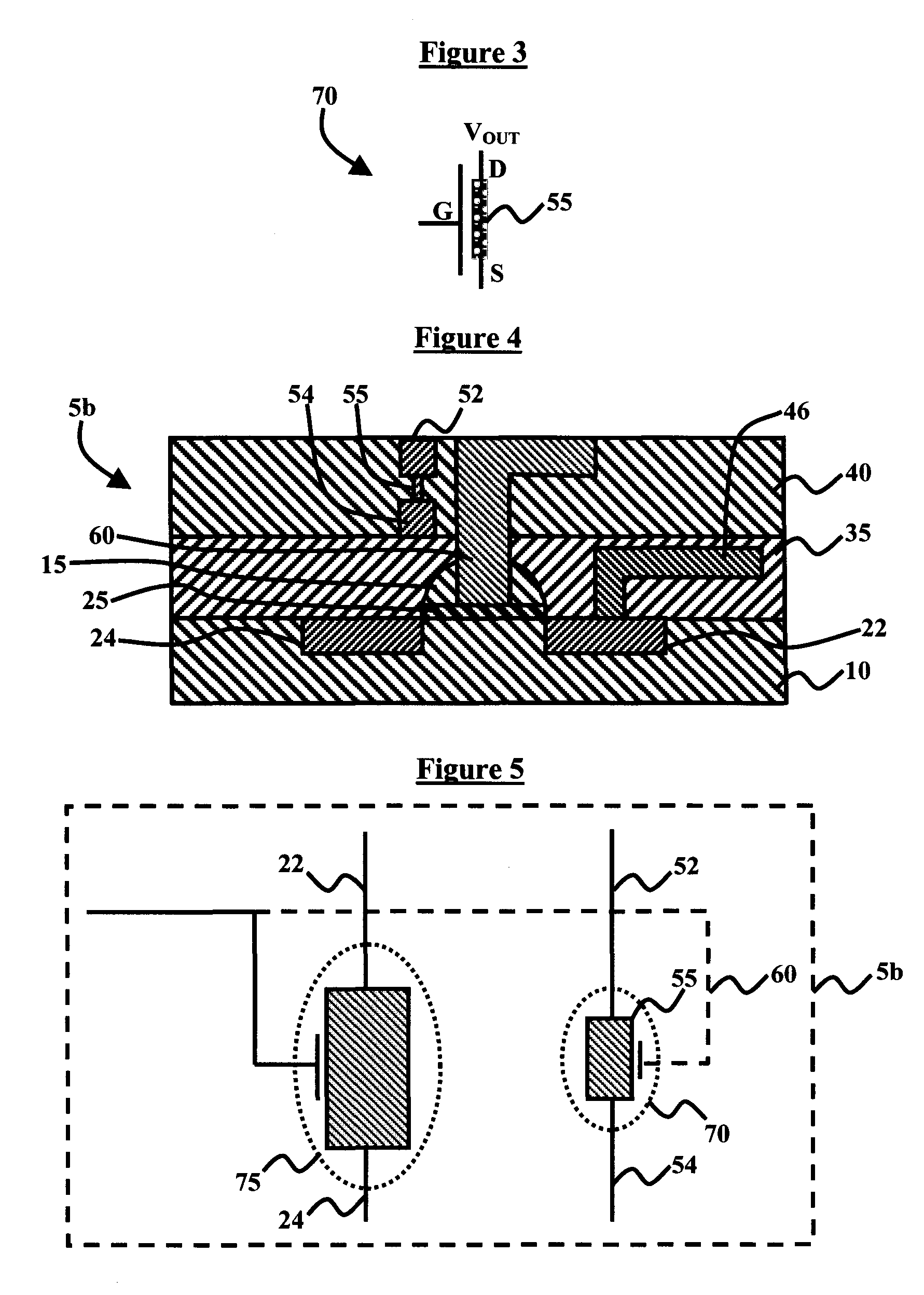
[0021]The embodiments of the invention and the various features and advantageous details thereof are explained more fully with reference to the non-limiting embodiments that are illustrated in the accompanying drawings and detailed in the following description. It should be noted that the features illustrated in the drawings are not necessarily drawn to scale. Descriptions of well-known components and processing techniques are omitted so as to not unnecessarily obscure the embodiments of the invention. The examples used herein are intended merely to facilitate an understanding of ways in which the embodiments of the invention may be practiced and to further enable those of skill in the art to practice the embodiments of the invention. Accordingly, the examples should not be construed as limiting the scope of the embodiments of the invention.

[0022]As mentioned, there remains a need for a novel structure and method for monitoring the operation of an integrated circuit during operation...


PUM


Abstract

A method and structure for an integrated circuit comprising a first transistor and an embedded carbon nanotube field effect transistor (CNT FET) proximate to the first transistor, wherein the CNT FET is dimensioned smaller than the first transistor. The CNT FET is adapted to sense signals from the first transistor, wherein the signals comprise any of temperature, voltage, current, electric field, and magnetic field signals. Moreover, the CNT FET is adapted to measure stress and strain in the integrated circuit, wherein the stress and strain comprise any of mechanical and thermal stress and strain. Additionally, the CNT FET is adapted to detect defective circuits within the integrated circuit.

Description

BACKGROUND OF INVENTION[0001]1. Field of the Invention[0002]The embodiments of the invention generally relate to integrated circuit technology, and more particularly to devices and techniques for evaluating operation parameters of integrated circuit chips.[0003]2. Description of the Related Art[0004]In the integrated circuit industry, it is imperative to monitor the operation of an integrated circuit for control, testing, and / or diagnostic purposes. Conventionally, signals are made either internally using electrical readouts (e.g., diagnostic circuits, latches, scan chains, and related structures), or remotely using physical sensors (e.g., charge coupling device (CCD) detectors, thermal imagers, and magnetic field sensors). Unfortunately, electrical readout circuitry generally occupies valuable chip area, induces performance degradation or load to critical circuits on the chip, and cannot specifically pinpoint the location of problems.[0005]Furthermore, remote sensing using physical...

Claims


Application Information

Patent Timeline
Patent Type & Authority Patents(United States)
IPC IPC(8): H01L31/072H01L23/48
CPCB82Y10/00G01R31/2884H01L27/286H01L29/0665H01L29/0673H01L51/0512H01L27/088H01L29/78H01L51/0048Y10S977/762Y10S977/761Y10S977/765H10K19/20H10K85/221H10K10/462
Inventor HAKEY, MARK C.MASTERS, MARK E.PASTEL, LEAH M. P.VALLETT, DAVID P.
Owner INT BUSINESS MASCH CORP
Why Eureka
Try Eureka