Method of deciding error rate and semiconductor integrated circuit device

a technology of error rate and integrated circuit, which is applied in the direction of redundant data error correction, instruments, digital storage, etc., can solve the problems of insufficient study of how to form a judgment, the inability to determine whether the number of erroneous rows disappears, etc., to achieve high reliability, reduce power consumption for an operation, and high reliability of a memory circuit

Inactive Publication Date: 2007-07-24
LONGITUDE LICENSING LTD
View PDF12 Cites 84 Cited by
  • Summary
  • Abstract
  • Description
  • Claims
  • Application Information

AI Technical Summary

Benefits of technology

[0009]It is thus an object of the present invention addressing the problems described above to provide a method of determining a data error rate with a high degree of reliability and to provide a semiconductor integrated circuit device having reduced power consumption for an operation to sustain information while assuring high reliability of a memory circuit comprising dynamic memory cells.

Problems solved by technology

There is no sufficient study of how to form a judgment on an erroneous row count detected by the error correction compound circuit to be used in controlling the frequency of refresh cycles as is the case with prior art 1.
In this case, it is impossible to determine whether the number of erroneous rows disappears as a result of the shortening of the refresh period or the number of erroneous rows disappears due to the fact that the number of erroneous rows is concentrated at the beginning of a refresh operation.
Thus, the memory cells' power to sustain data is not determined correctly.
If the number of erroneous rows is compared with the allowable limit after the refresh operation is completed for all memory cells, however, a problem caused by an erroneous row count far exceeding the allowable limit after the refresh operation can no longer be solved.
As a result, the expected reliability of the error correction cannot be assured anymore.

Method used


Image

  • Method of deciding error rate and semiconductor integrated circuit device
  • Method of deciding error rate and semiconductor integrated circuit device
  • Method of deciding error rate and semiconductor integrated circuit device

Examples


Embodiment Construction

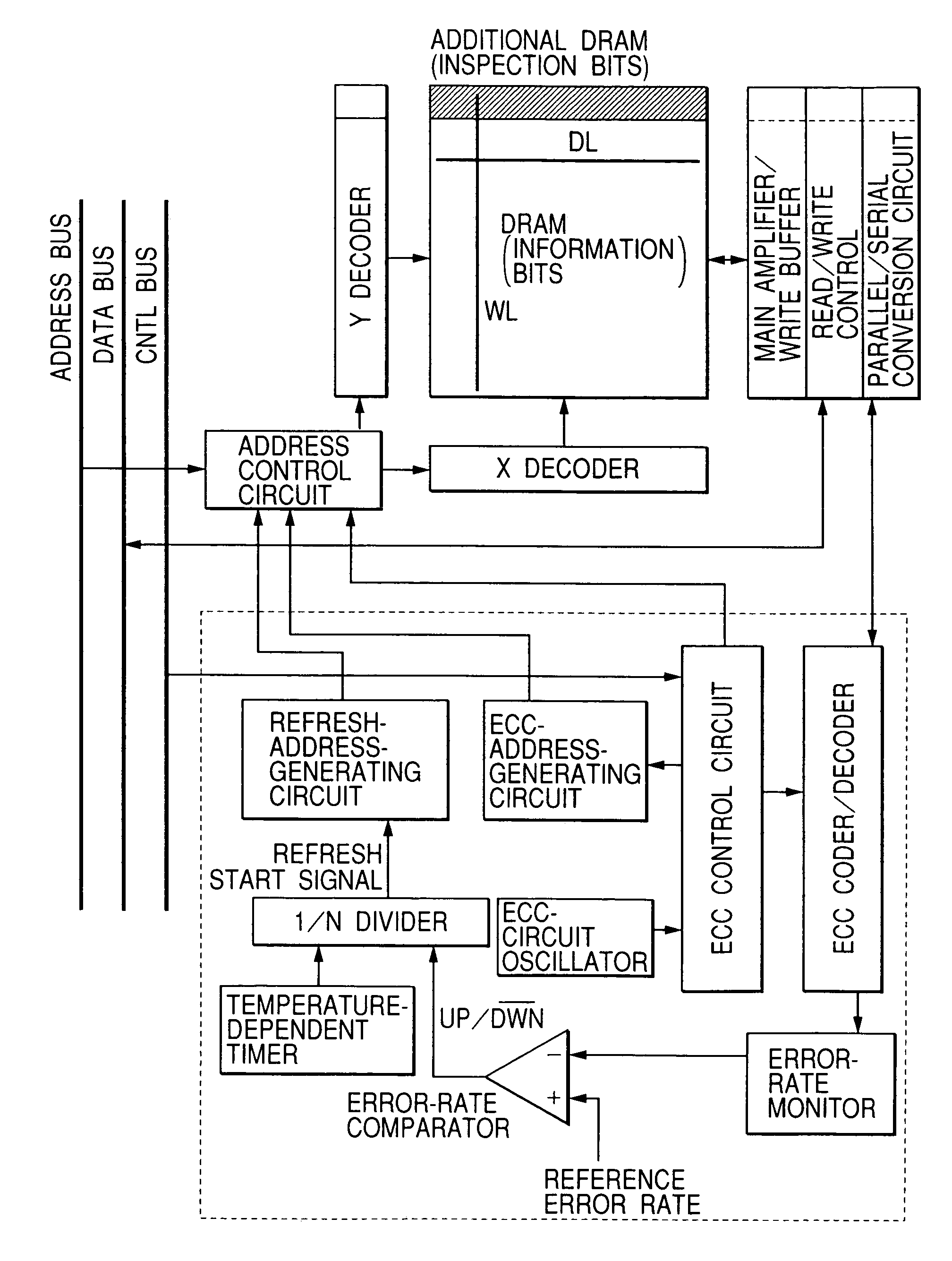
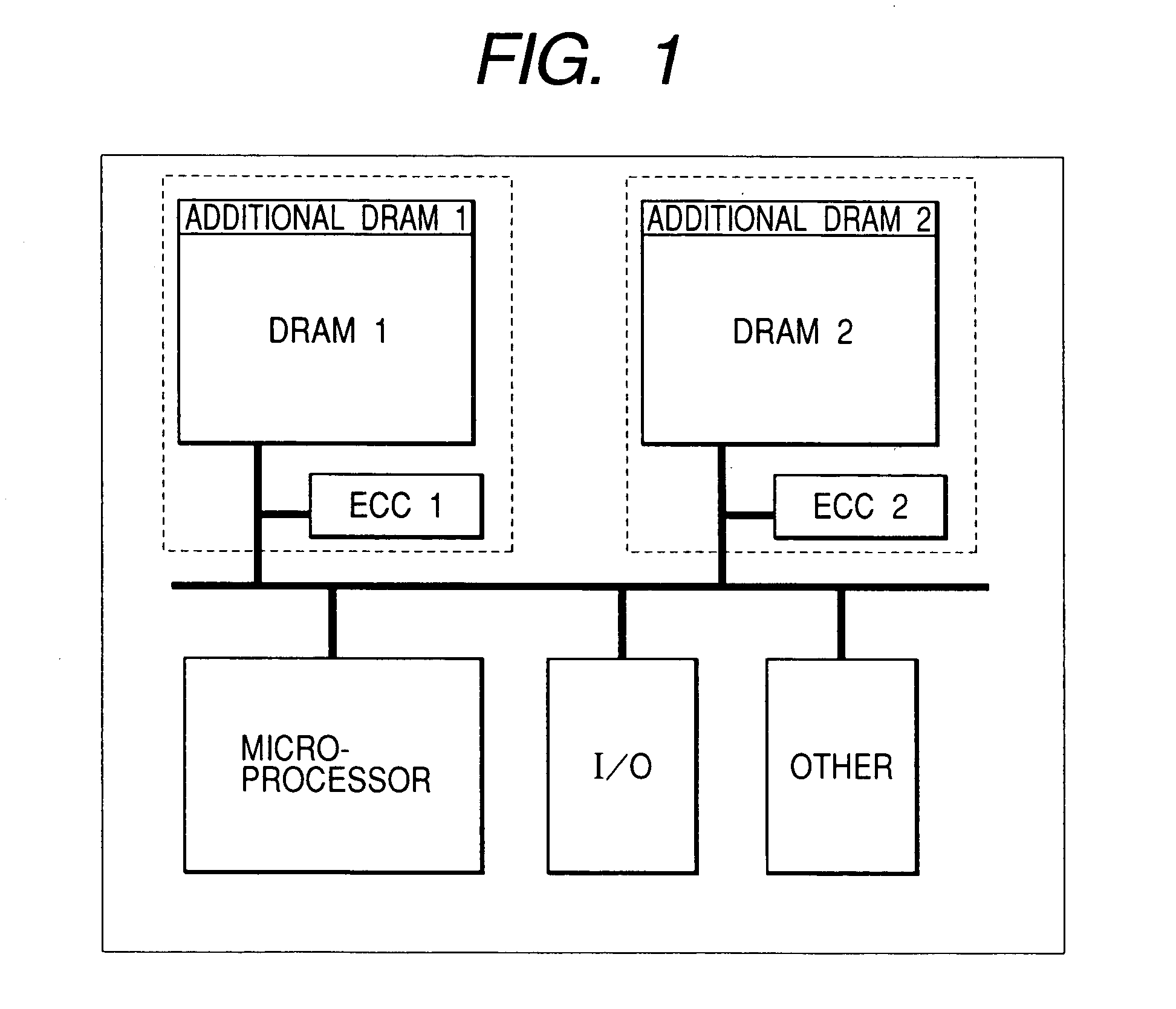
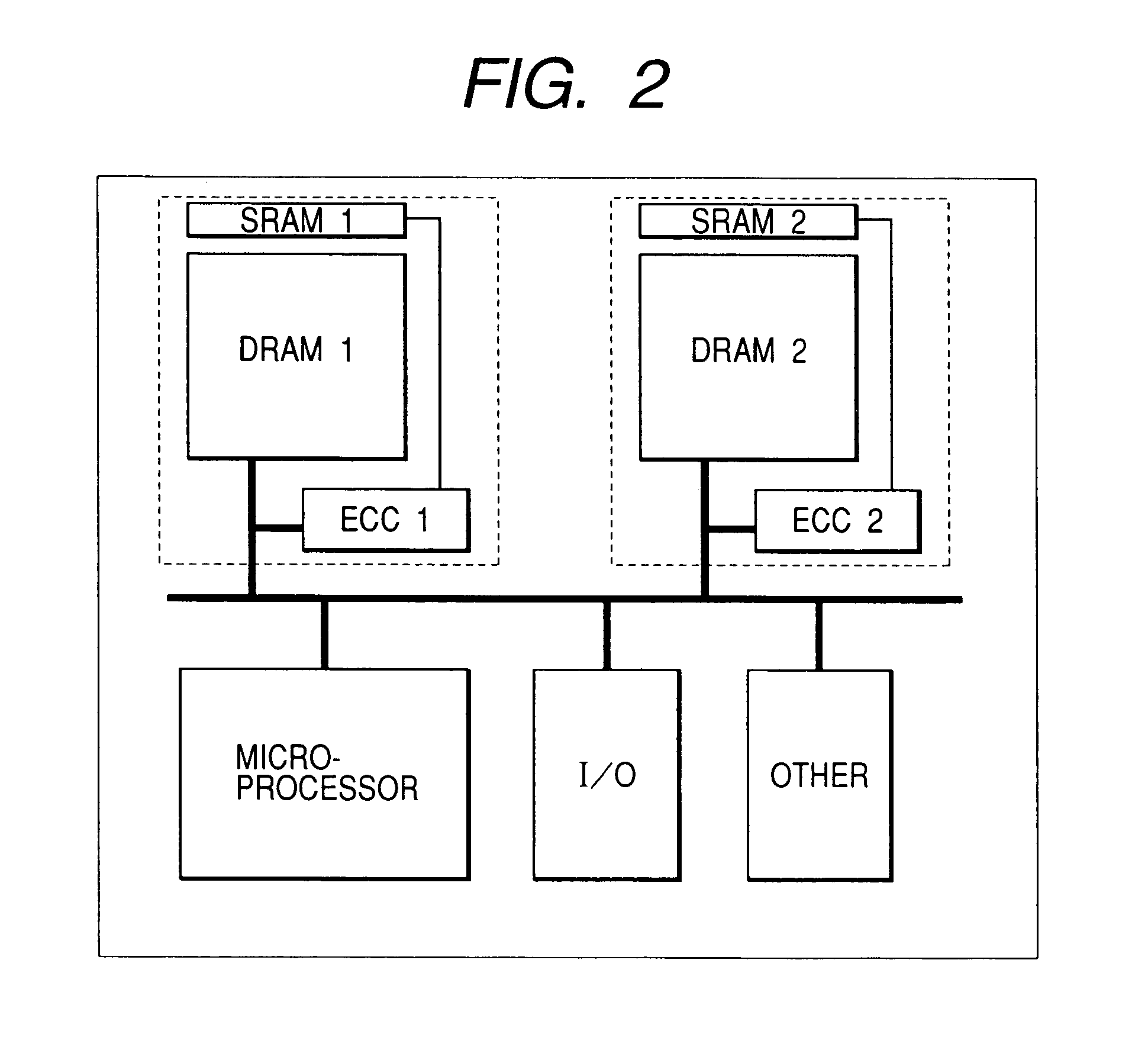
[0044]FIG. 1 shows the configuration of an embodiment implementing a system LSI provided by the present invention. Each circuit block shown in the figure is created on a single semiconductor substrate made of typically monocrystalline silicon by adoption of a generally known technology of manufacturing a semiconductor integrated circuit. The embodiment has embedded memory circuits including ordinary DRAM (Dynamic Random Access Memory) 1, ordinary DRAM 2, additional DRAM 1, additional DRAM 2, ECC (Error Checking and Correction) circuit ECC 1 and ECC circuit ECC 2, which are shown in the figure as representative memory circuits. In this embodiment, ordinary DRAM 1 and ordinary DRAM 2 form a pair. So do additional DRAM 1 and additional DRAM 2 as well as ECC circuit ECC 1 and ECC circuit ECC 2. Of course, it is also possible to provide only ordinary DRAM 1 or ordinary DRAM 2, additional DRAM 1 or additional DRAM 2 and ECC circuit ECC 1 or ECC circuit ECC 2. As an alternative, a common E...


PUM


Abstract

An error rate select circuit activated in an information sustaining mode is provided, wherein a plurality of pieces of data are read from a dynamic memory circuit and inspection bits which are used to detect an error existing in the pieces of data are generated. If no error is detected, a first predetermined value is added to a total value. If an error is detected, a second predetermined value greater than the first predetermined value is subtracted from the total value. If the total value exceeds a first set value, a refresh period is lengthened by a predetermined time increment. If the total value becomes smaller than a second set value, the refresh period is shortened by the predetermined time increment.

Description

CROSS-REFERENCE TO RELATED APPLICATION[0001]This application is a division of application Ser. No. 09 / 875,961 filed Jun. 8, 2001 now U.S. Pat. No. 6,735,726.BACKGROUND[0002]In general, the present invention relates to a method of determining an error rate and a semiconductor integrated circuit device. More particularly, the present invention relates to an effective technology such as a data holding technology adopted in a memory circuit comprising dynamic memory cells.[0003]As a result of a survey conducted after the present invention, Unexamined Patent Publication No. Hei 11(1999)-213659 and Unexamined Patent Publication No. Hei 7(1995)-262794 were identified. Referred to hereafter as prior art 1 and prior art 2 respectively, the former and latter publications are considered to be relevant to the present invention described later in this specification. Prior art 1 is a technology to control the frequency of refresh cycles by a CPU through execution of software using the number of e...

Claims


Application Information

Patent Timeline
Patent Type & Authority Patents(United States)
IPC IPC(8): G06F11/00G06F11/10G11C7/10G11C11/406G11C11/401G11C29/08G11C29/42
CPCG06F11/1008G11C7/1006G11C29/42G06F2201/88G06F2211/109
Inventor MURANAKA, MASAYAKATO, HIDEAKIITO, YUTAKA
Owner LONGITUDE LICENSING LTD
Why Eureka
Try Eureka