
Erase algorithm for multi-level bit flash memory

a multi-level bit flash memory and erase algorithm technology, applied in static storage, digital storage, instruments, etc., can solve the problems of reducing speed and cost, and reducing data storage density, etc., to achieve greater density and ease of erasability. , the effect of reducing the number of times

Active Publication Date: 2007-07-31
SPANSION LLC
View PDF7 Cites 21 Cited by
  • Summary
  • Abstract
  • Description
  • Claims
  • Application Information

AI Technical Summary

Benefits of technology

The algorithm achieves highly compact threshold voltage distributions, enhancing memory device density, speed, and reliability while minimizing erase time and power consumption, thereby improving the performance and capacity of flash memory devices.

Problems solved by technology

For example, DRAM and SRAM allow individual bits of data to be erased one at a time, but such memory loses its data when power is removed.
EEPROM can alternatively be easily erased without extra exterior equipment, but has reduced data storage density, lower speed, and higher cost.
EPROM, in contrast, is less expensive and has greater density but lacks ease of erasability.
With such an erase procedure, however, some cells may become “over-erased” before other cells are sufficiently erased.
For several reasons it is undesirable for a memory cell to remain in an over-erased condition.
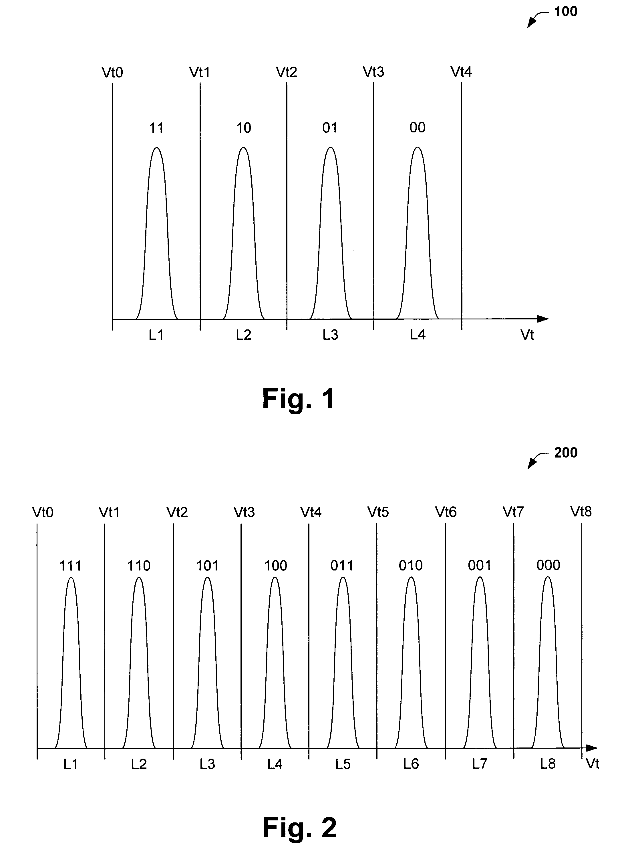
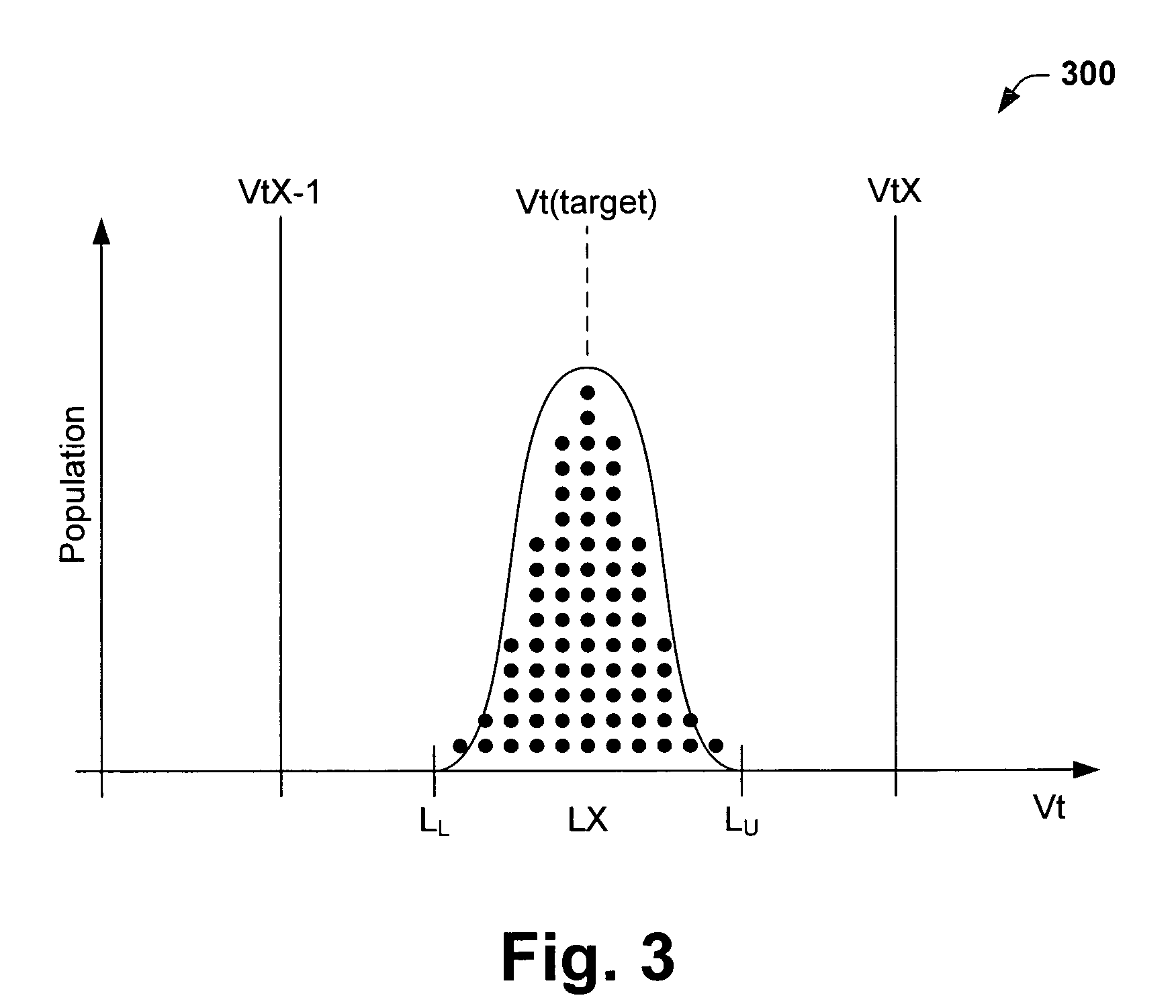
Regardless of the flash architecture employed, accurately erasing and programming multiple level flash cells can be particularly sensitive with the attendant complications of maintaining narrow Vt distributions in order to accurately read and determine a data state from a corresponding Vt level.
In addition, even if such narrow distributions are attained for the various multiple levels, unless sectors of memory cells can be erased to within the acceptable limits quickly, efficiently, and reliably, little competitive advantage may be gained.

Method used


Image

  • Erase algorithm for multi-level bit flash memory
  • Erase algorithm for multi-level bit flash memory
  • Erase algorithm for multi-level bit flash memory

Examples


Embodiment Construction

[0027]One or more aspects of the present invention are described with reference to the drawings, wherein like reference numerals are generally utilized to refer to like elements throughout, and wherein the various structures are not necessarily drawn to scale. In the following description, for purposes of explanation, numerous specific details are set forth in order to provide a thorough understanding of one or more aspects of the present invention. It may be evident, however, to one skilled in the art that one or more aspects of the present invention may be practiced with a lesser degree of these specific details. In other instances, well-known structures and devices are shown in block diagram form in order to facilitate describing one or more aspects of the present invention.

[0028]Improvements in the density of memory devices translate to increased memory capacity. Density and thus capacity is a major consideration in the cost of fabrication and the marketability of memory devices...


PUM


Abstract

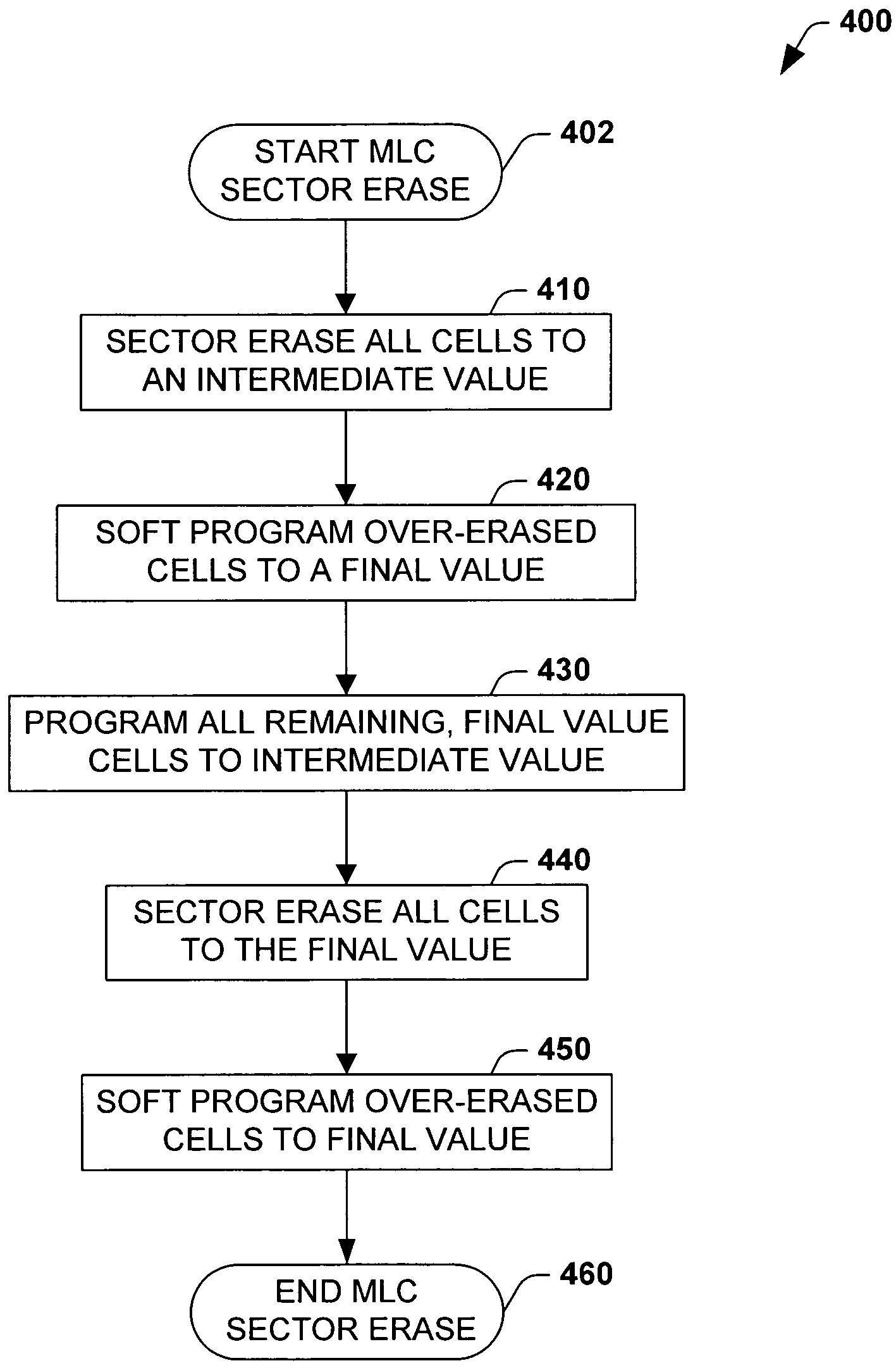
Methods of erasing a sector of multi-level flash memory cells (MLB) having three or more data states to a single data state are provided. The present invention employs an interactive sector erase algorithm that repeatedly erases, verifies, soft programs, and programs the sector in two or more erase phases to achieve highly compact data state distributions. In one example, the algorithm essentially erases all the MLB cells of the sector to an intermediate state and corresponding threshold voltage value using interactive erasing, soft programming and programming pulses in a first phase. Then in a second phase, the algorithm further erases all the MLB cells of the sector using additional interactive erasing and soft programming pulses until a final data state is achieved corresponding to a desired final threshold voltage value of the cells. Optionally, the algorithm may include one or more additional phases of similar operations that successively bring the memory cells of the sector to a compacted common erased state in preparation for subsequent programming operations. In one aspect of the method, the actual threshold values and / or data states chosen for these phases may be predetermined and input to the memory device by the user.

Description

FIELD OF INVENTION[0001]The present invention relates generally to memory devices and the like, and in particular to a method of erasing sectors of cells with multiple-level data states in flash memory devices.BACKGROUND OF THE INVENTION[0002]Many different types and styles of memory exist to store data for computers and similar type systems. For example, random access memory (RAM), dynamic random access memory (DRAM), static random access memory (SRAM), read only memory (ROM), programmable read only memory (PROM), electrically programmable read only memory (EPROM), electrically erasable programmable read only memory (EEPROM) and flash memory are all presently available to accommodate data storage.[0003]Each type of memory has its own particular advantages and disadvantages. For example, DRAM and SRAM allow individual bits of data to be erased one at a time, but such memory loses its data when power is removed. EEPROM can alternatively be easily erased without extra exterior equipme...

Claims


Application Information

Patent Timeline
Patent Type & Authority Patents(United States)
IPC IPC(8): G11C11/34G11C11/56G11C16/34
CPCG11C11/5635G11C16/3404G11C16/3409G11C16/3413G11C11/56G11C16/34G11C16/02G11C16/10
Inventor HSIA, EDHAMILTON, DARLENEBATHUL, FATIMAHORIIKE, MASATO
Owner SPANSION LLC
Learn More