Data processing apparatus that shares a single semiconductor memory circuit among multiple data processing units

a data processing apparatus and data processing technology, applied in the direction of data conversion, pulse automatic control, generating/distributing signals, etc., can solve the problems of reducing the overall operating speed, reducing the overall circuit scale, and switching delay

Inactive Publication Date: 2007-08-07
RENESAS ELECTRONICS CORP
View PDF12 Cites 23 Cited by
  • Summary
  • Abstract
  • Description
  • Claims
  • Application Information

AI Technical Summary

Benefits of technology

[0017]According to another aspect of the embodiments, a semiconductor memory can enter a lower power

Problems solved by technology

However, such a circuit increases overall circuit scale (e.g., size).
Further, the bus control circuit 104 can decrease overall operating speed, as such a circuit introduces a switching delay into data access operations.
However, such an approach may be difficult to implement.
This can re

Method used


Image

  • Data processing apparatus that shares a single semiconductor memory circuit among multiple data processing units
  • Data processing apparatus that shares a single semiconductor memory circuit among multiple data processing units
  • Data processing apparatus that shares a single semiconductor memory circuit among multiple data processing units

Examples


Embodiment Construction

[0039]Various embodiments of the present invention will now be described in detail with reference to accompanying drawings. The examples described below can include various constituents that are identical, or essentially the same as those of the conventional data processing apparatus shown in FIG. 4.

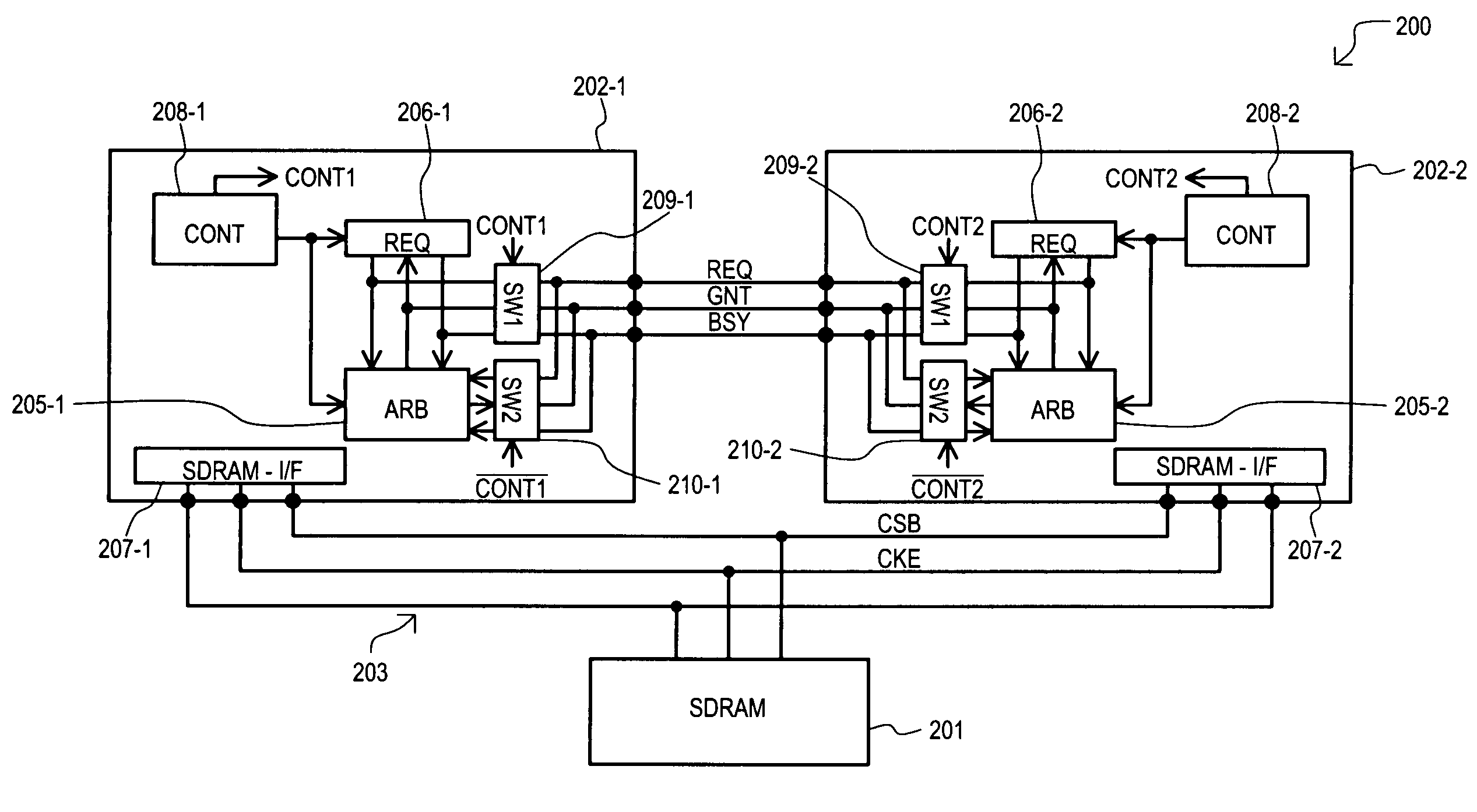
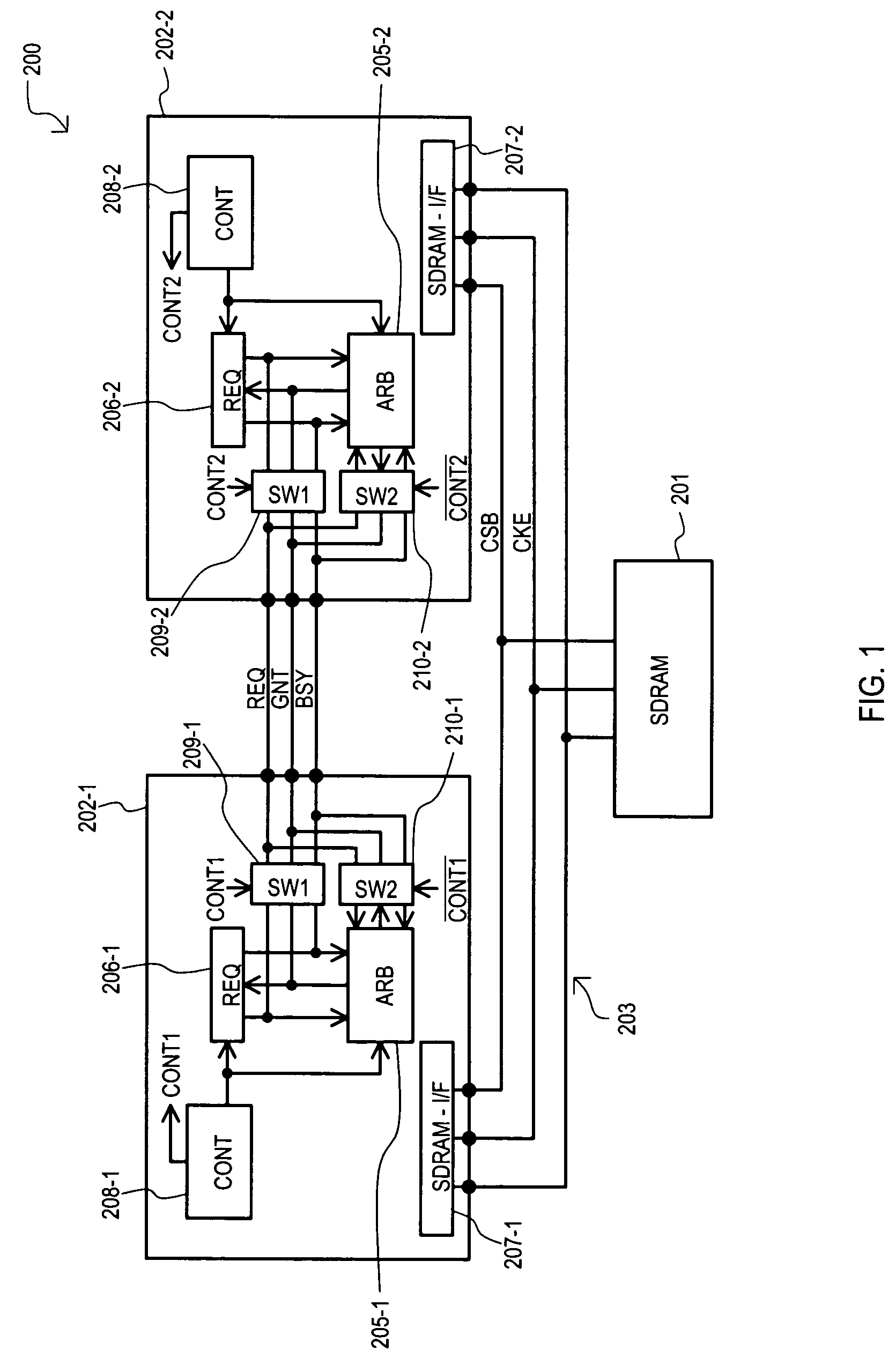
[0040]Referring now to FIG. 1, a data processing apparatus according to one embodiment of the present invention is set forth in block schematic diagram and designated by the general reference character 200. A data processing apparatus 200 can include a semiconductor memory circuit, which in this case is a DDR-SDRAM 201, and data processing circuits 202-1 and 202-2. Data processing circuits (202-1 and 202-2) can be connected with DDR-SDRAM 201 by way of system bus 203.

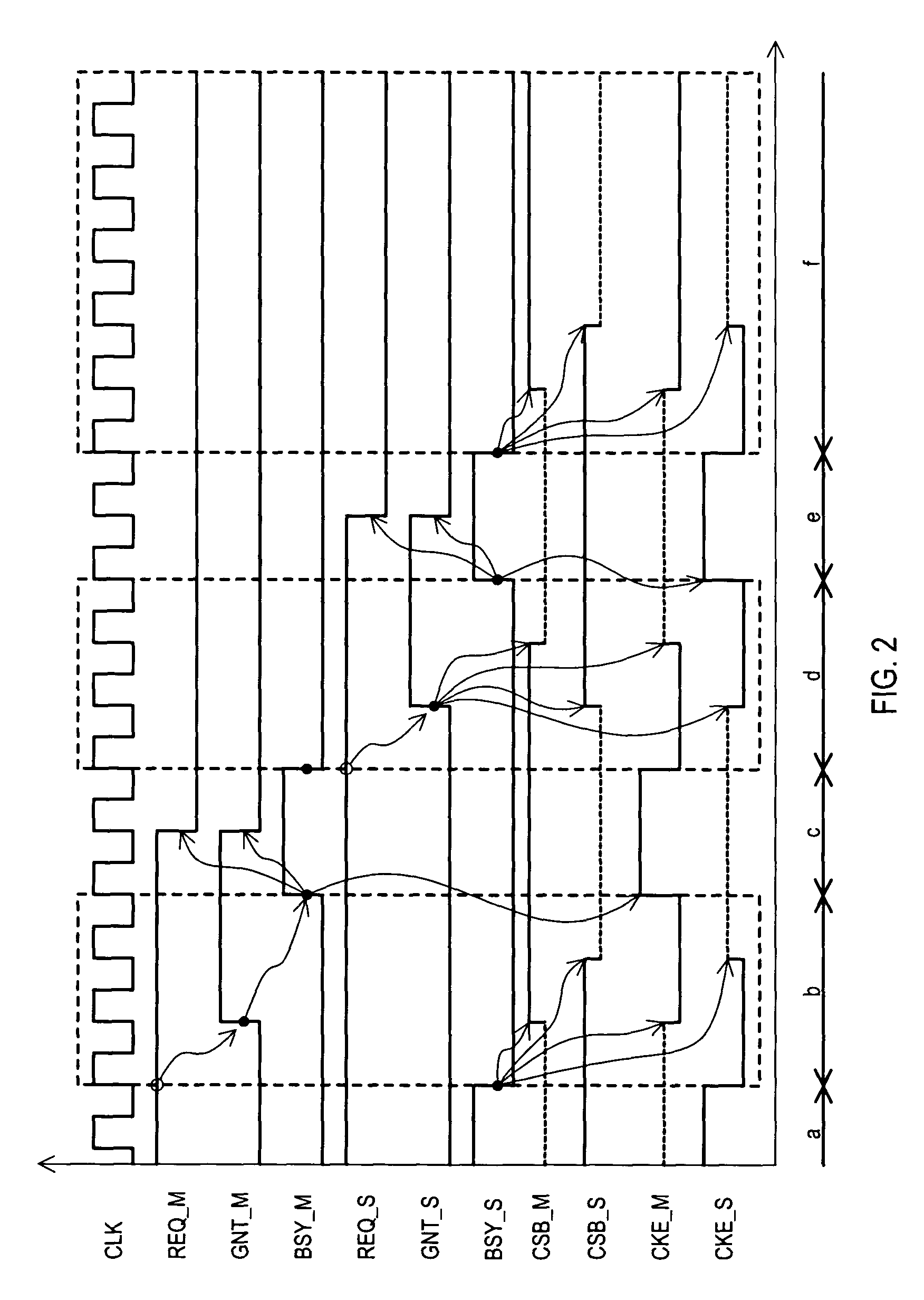
[0041]System bus 203 can transmit a chip select signal CSB, a clock enable signal CKE, and other signals (including command and address signals). In addition, it is assumed that a clock oscillator (not shown) for data proces...


PUM


Abstract

Multiple data processing circuits may share a semiconductor memory circuit, such as double-data-rate synchronous dynamic random access memory (DDR-SDRAM). A data processing circuit (202-1 or 202-2) ending control of a semiconductor memory circuit (201) supplies a clock enable signal and chip select signal at predetermined levels. A data processing circuit (202-2 or 202-1) starting control of a semiconductor memory circuit (201) supplies a clock enable signal and chip select signal at the same predetermined levels, before the data processing circuit (202-1 or 202-2) ending control stops supplying a clock enable signal and chip select signal. Therefore, a clock enable signal and chip select signal do not enter an undefined state, and malfunctions that could otherwise occur are prevented.

Description

TECHNICAL FIELD[0001]The present invention relates to generally to a data processing apparatus that includes a semiconductor circuit and a data processing circuit, and more particularly to a data processing apparatus in which a semiconductor memory circuit is shared among multiple data processing circuits.BACKGROUND OF THE INVENTION[0002]Conventionally, a data processing apparatus is known that uses a sharing arbitration circuit. The sharing arbitration circuit can arbitrate the sharing of a semiconductor memory circuit among multiple data processing circuits. Examples of such conventional data processing apparatuses are shown in Japanese Patent Publication JP 06-83780A, JP 11-272632A, and JP 2000-298652A.[0003]Referring to FIG. 4, a conventional example of a data processing apparatus described above is shown, and designated by the general reference character 100. A data processing apparatus 100 can include a synchronous dynamic random access memory (SDRAM) 101 provided as a semicon...

Claims


Application Information

Patent Timeline
IPC IPC(8): G06F12/00G06F13/42
CPCG06F13/4243
Inventor UNEME, MASAKATSU
Owner RENESAS ELECTRONICS CORP
Why Eureka
Try Eureka