Optoelectronic waveguiding device, structural body including the same, and optical module

a waveguide device and waveguide technology, applied in the direction of optical elements, instruments, semiconductor lasers, etc., can solve the problems of increasing the operating current, deteriorating the reliability of the device, increasing the stress, etc., and achieves the effect of suppressing the reaction, dissipating heat from an active region, and reducing the stress

Inactive Publication Date: 2007-08-14
LUMENTUM JAPAN INC
View PDF8 Cites 7 Cited by
  • Summary
  • Abstract
  • Description
  • Claims
  • Application Information

AI Technical Summary

Benefits of technology

[0011]The inventors of the present invention provide a structure which not only suppresses reaction between the electrode metal of an optical device and the solder metal of a mounting plate but also satisfactorily dissipate heat from an active region. Specifically, the surface of the optical device is partially coated with a dielectric film and the optical device is mounted on the solder metal with a waveguide of the optical device bought into contact with the solder metal so that the reaction between the solder metal and the electrode of the optical device can be suppressed in the vicinity of the waveguide of the optical device without deteriorating the thermal dissipation performance. This makes it unnecessary to increase the operating current.
[0012]The present invention solves the above-mentioned problem of increasing the operating current of an optical device by improving the thermal conductivity and therefore provides a highly reliable device. According to the present invention, the central part of the electrode of the optical device is coated with a dielectric film. The optical device is mounted junction down to a mounting plate in such a manner that the optical device is in contact with the solder metal of the mounting plate via the one dielectric film. As a result of avoiding direct contact between the solder metal of the mounting plate and the electrode of the optical device, it is possible to suppress reaction between the solder metal and the electrode of the optical device. In addition, since the mounting plate is in contact with the optical device in view of thermal dissipation or thermal conductivity, its thermal conductivity is better than the above-mentioned one provided with the void. As a result, it is possible to suppress temperature rise in the active region during operation of the device and therefore reduce the operating current of the device.
[0013]In addition, since the electrode of the device is provided with the layer which suppresses reaction with the solder metal, restrictions on the electrode are mitigated. For example, although such a metal as Ti or Pt is usually deposited to prevent penetration of the solder metal, its thickness can be reduced to a minimum. It is therefore possible to prevent Ti or Pt from causing stress. This reduces the stress which acts on the active layer or optical absorption layer of the device and which deteriorates the reliability of the device.
[0014]The largest effect of the present invention is obtained when the present invention is applied to a non-hermetically packaged optical module. In a non-hermetically packaged optical module, external moisture may penetrate the package of the optical module. Water molecules in the package oxidize the solder metal and the surface electrode of the optical device. This oxidization causes increased stresses and diffused metal atoms and therefore deteriorates the optical device. If the present invention is applied, abnormal reaction between the solder metal and the surface electrode of the optical device can be suppressed since the surface of the electrode is protected with a dielectric film.

Problems solved by technology

This makes it unnecessary to increase the operating current.
This reduces the stress which acts on the active layer or optical absorption layer of the device and which deteriorates the reliability of the device.
This oxidization causes increased stresses and diffused metal atoms and therefore deteriorates the optical device.

Method used


Image

  • Optoelectronic waveguiding device, structural body including the same, and optical module
  • Optoelectronic waveguiding device, structural body including the same, and optical module
  • Optoelectronic waveguiding device, structural body including the same, and optical module

Examples


embodiment 1

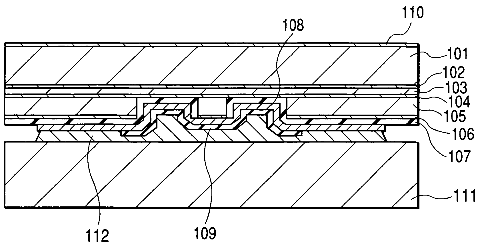
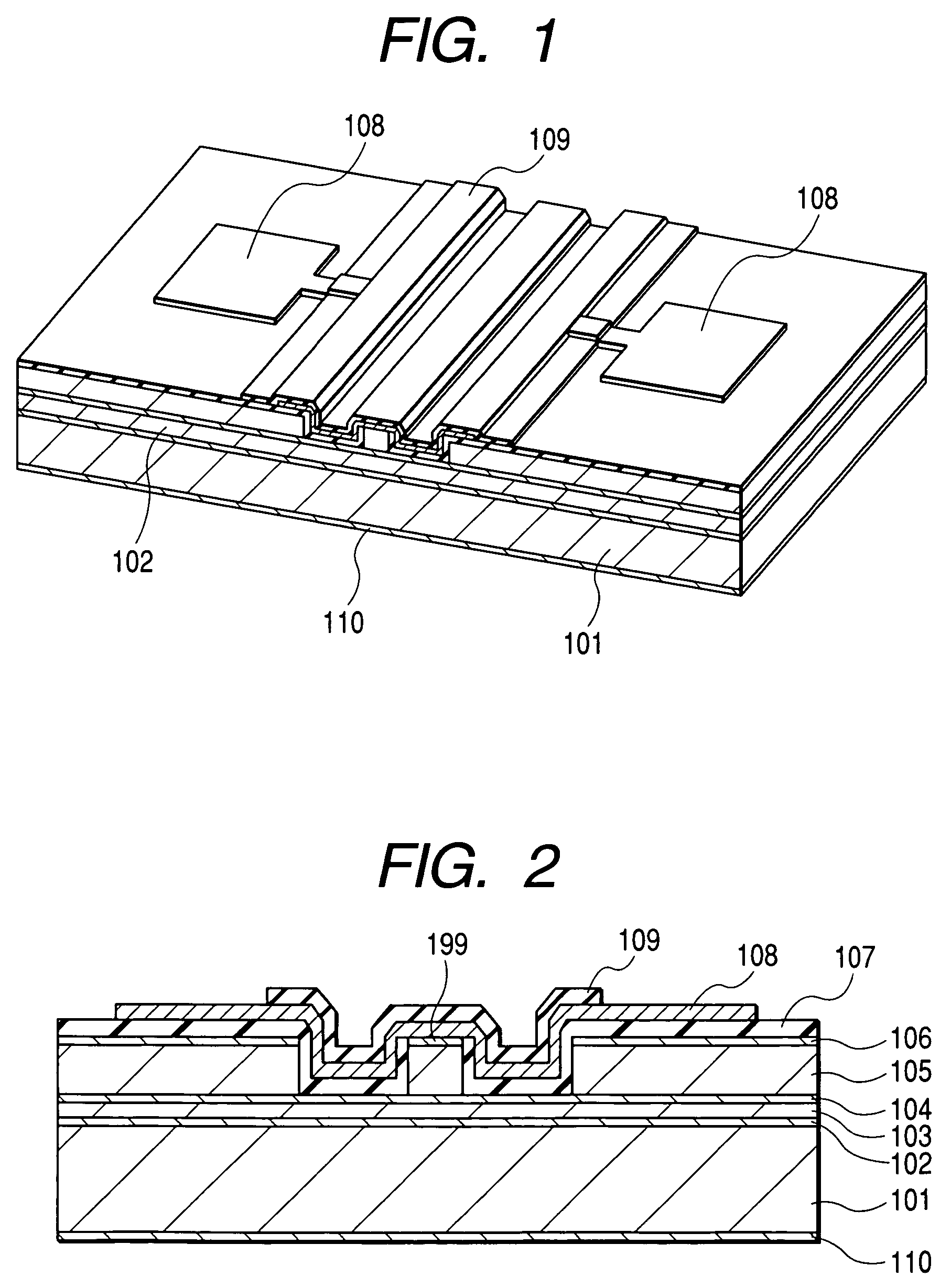
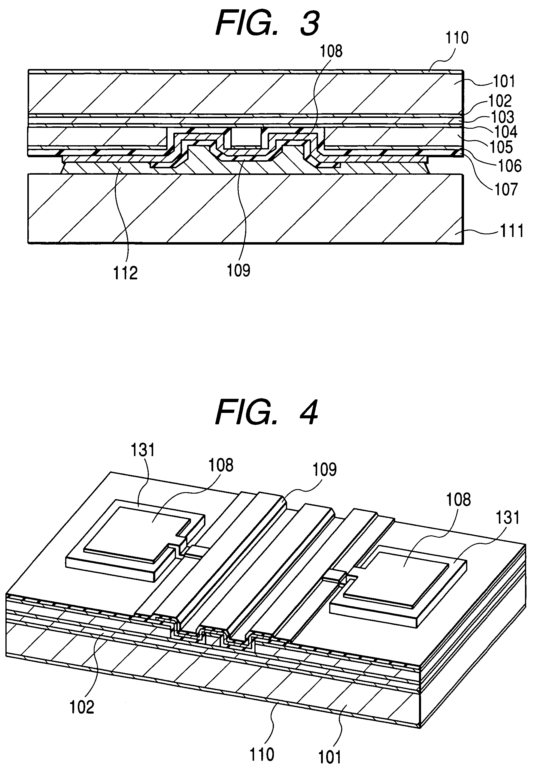
[0030]The following will describe a ridge waveguide type Fabry-Perot (F-P) laser according to a first embodiment of the present invention. FIG. 1 is a perspective view of the first embodiment of the present invention and FIG. 2 is a sectional view of the optical waveguide. The device is a ridge waveguide type laser with an active layer made of InGaAsP-based material. On an n-type InP substrate 101 with a plane direction (100), an n-type InGaAsP optical confinement layer 102, a multi-quantum well layer 103 and a p-type InGaAsP optical confinement layer 104 are formed. Further, on the top of it, a p-type InP clad layer 105 and a p-type InGaAs ohmic contact layer 106 are stacked. The quantum well layer is formed as an active region by stacking seven pairs (periods) of a 6 nm-thick well layer and a 10 nm-thick barrier layer so as to set the oscillating wavelength to about 1300 nm. Although InGaAsP-based material is used as the material of the active region in this embodiment, InGaAlAs-b...

embodiment 2

[0040]The following describes a BH (Buried Heterostructure) type laser as a second embodiment of the present invention. FIGS. 7 and 8 are its perspective view and sectional view, respectively. The layered structure of the laser is the same as in the first embodiment. On an n-type InP substrate 201 with a plane direction (100), a InGaAsP-based active layer 202, a p type InP clad layer 203 and a p type ohmic contact layer 204 are stacked in this order. The active layer is composed of an InGaAsP optical confinement layer, a multi-quantum well layer and a p type InGaAsP optical confinement layer. The active layer is designed to set the oscillating wavelength to about 1300 nm. The oscillating wavelength must not be set to 1300 nm. The active layer may also be design to have a different oscillating wavelength as desired.

[0041]Using the wafer on which a desired layer structure is stacked, a BH type laser is fabricated by a known method. The active region is buried in Fe-added semi-insulati...

embodiment 3

[0044]FIGS. 10 and 11 show a VCSEL (Vertical Cavity Surface Emitting Laser) according to a third embodiment of the present invention. FIG. 11 is a sectional view of the vertical cavity surface emitting laser mounted on a mounting plate 301 via a solder metal 302. On an n-type GaAs substrate 311 with a plane direction (100), Bragg reflectors 312 and 313 and an active layer 314 are stacked. The structure consisting of the active region and Bragg reflectors is the same as a widely known structure and therefore not described here in detail. After the layered structure is formed, a current confinement structure, a surface dielectric film 315 and a p-side electrode 316 are formed. Further, the electrode is partially coated with a dielectric film 317 in order to prevent reaction with the solder metal of a mounting plate onto which the device is to be mounted. This coating of the electrode with the dielectric film 317 can prevent reaction between the electrode and the solder metal in the vi...


PUM


Abstract

The semiconductor optical device is mounted junction down on a mounting plate via the solder metal of the mounting plate. The electrode of the semiconductor optical device facing the mounting plate is partially coated with a dielectric film and the dielectric film is in contact with the solder metal on the mounting plate.The reaction between the semiconductor optical device and the solder metal of the mounting plate can be suppressed without deteriorating the thermal conductivity between the semiconductor optical device and the mounting plate. Therefore, it is possible to improve the reliability of the semiconductor optical device mounted in the junction down form since diffusion of the solder metal into the semiconductor can be prevented.

Description

BACKGROUND OF THE INVENTION[0001]1. Field of the Invention[0002]The present invention relates to structure of an optical device, such as a semiconductor laser, and structure for mounting the optical device.[0003]2. Related Art[0004]In an optical fiber communication system, optical modules occupy a large part of the parts cost. To lower the price of an optical module, in particular, it is very significant to simplify the mounting of the optical device in the optical module. Accordingly, there have been several simple mounting methods known widely. Their mainstream is to mount a semiconductor laser junction down on a simple mount in an optical module. For example, such simple mounting structures were reported in the 1997 General Conference of the Institute of Electronics, Information and Communication Engineers, Proceedings, Lecture Nos. C3-65, CS-68, etc.[0005]When a semiconductor laser is mounted junction down, the semiconductor laser is bonded to a simple optical device mounting pl...

Claims


Application Information

Patent Timeline
Patent Type & Authority Patents(United States)
IPC IPC(8): H01S5/00G02B6/12H01S3/04H01S5/028H01S5/02H01S5/022H01S5/024H01S5/042H01S5/183H01S5/22H01S5/343
CPCB82Y20/00H01S5/0224G02B2006/12097H01S5/02272H01S5/024H01S5/18308H01S5/22H01S5/34306H01S2301/176H01S5/0234H01S5/0237
Inventor SATO, HIROSHIAOKI, MASAHIROTSUJI, SHINJI
Owner LUMENTUM JAPAN INC
Why Eureka
Try Eureka