Interconnects for solar cell devices

a solar cell and solar cell technology, applied in the field of solar cell assemblies, can solve the problems of reducing the efficiency of increasing the occurrence of pinholes and similar flaws in larger planar solar cells, and increasing the cost of making crystalline silicon-based cells

Inactive Publication Date: 2007-08-21
SOLYNDRA RESIDUAL TRUST
View PDF57 Cites 145 Cited by
  • Summary
  • Abstract
  • Description
  • Claims
  • Application Information

AI Technical Summary

Problems solved by technology

However, because of the expense in making crystalline silicon-based cells, thin film solar cells made of materials other than silicon have been explored and used.
However, even when a TCO layer is present, a bus bar network 114 is typically needed to draw off current since the TCO has too much resistance to efficiently perform this function in larger solar cells.
Although such cells are highly efficient when they are smaller, larger planar solar cells have reduced efficiency because it is harder to make the semiconductor films that form the junction in such solar cells uniform.
Furthermore, the occurrence of pinholes and similar flaws increase in larger planar solar cells.
These features can cause shunts across the junction.
A number of problems are associated with solar cell designs present in the known art.
While device 210 is functional, it is unsatisfactory.
This results in a net loss in absorber area, making the solar cell less efficient.
Furthermore, such a junction is difficult to make relative to other solar cell designs.
While the solar cell disclosed in FIG. 3 is functional, it is also unsatisfactory.
The Weinstein and Lee solar cell has the drawback of being bulky and expensive to build.
However, S59-125670 has a number of significant drawbacks that limit the efficiency of the disclosed devices.
First, the manner in which current is drawn off the exterior surface is inefficient because layer 5 does not wrap all the way around the rod (e.g., see FIG. 3B).
Second, substrate 7 is a metal plate that does not permit the passage of light.
Such a leakage path reduces the efficiency of the solar cell.
For example, any such dark junction areas will result in a leakage that will detract from the photocurrent of the cell.
Another disadvantage with the design disclosed in FIGS. 3B and 3C is that the rods are arranged in parallel rather than in series.
Thus, the current levels in such devices will be large, relative to a corresponding serially arranged model, and therefore subject to resistive losses.
Thus, Twin Solar devices have the drawback that they are not truly bifacial.
The solar cell assembly is therefore inefficient because direct light cannot enter both sides of the assembly.

Method used


Image

  • Interconnects for solar cell devices
  • Interconnects for solar cell devices
  • Interconnects for solar cell devices

Examples


Embodiment Construction

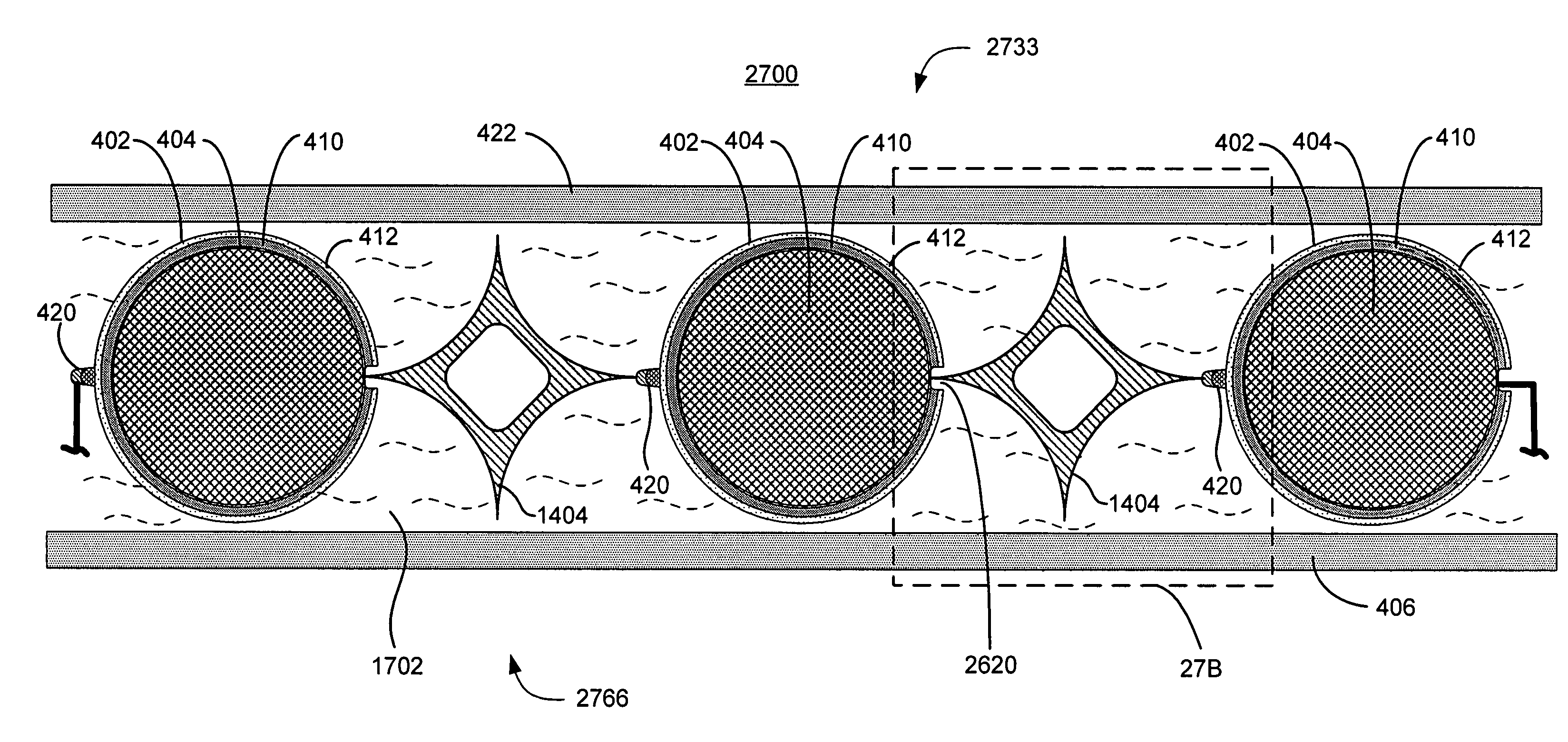
[0079]Disclosed herein are solar cell assemblies for converting solar energy into electrical energy and more particularly to improved solar cells and solar cell arrays. The solar cells of the present invention have a wire shape and are arranged in parallel but are electrically connected in series.

5.1 Basic Structure

[0080]The present invention provides a solar cell assembly 400 in which elongated solar cells 402, shown in cross-section in FIG. 4A, serve to absorb light. A conductive core (elongated conductive core) 404 serves as the first electrode in the assembly and a transparent conductive oxide (TCO) 412 on the exterior surface of each solar cell serves as the counter-electrode.

[0081]In general, conductive core 404 is made out of any material such that it can support the photovoltaic current generated by the solar cell with negligible resistive losses. In some embodiments, conductive core 404 is composed of any conductive material, such as aluminum, molybdenum, titanium, steel, n...


PUM


Abstract

A solar cell assembly comprising a plurality of elongated solar cells, each respective solar cell comprising (i) a core configured as a first electrode, (ii) a semiconductor junction circumferentially disposed on the core, (iii) a transparent conductive oxide (TCO) layer disposed on the semiconductor junction, and (iv) an elongated counter-electrode disposed lengthwise on a first side of the respective solar cell and extending outward from the TCO layer. On a second side of each cell, approximately opposite the counter-electrode, is a notch or other disruption extending through the semiconductor junction and the transparent oxide layer, thereby exposing the core of the solar cell. The solar cell assembly may further comprise conductive internal reflectors configured between a first and second elongated solar cell in the plurality of solar cells such that a portion of the solar light reflected from the respective internal reflector is reflected onto the solar cells.

Description

1. FIELD OF THE INVENTION[0001]This invention relates to solar cell assemblies for converting solar energy into electrical energy and more particularly to improved solar cell assemblies.2. BACKGROUND OF THE INVENTION[0002]Interest in photovoltaic cells has grown rapidly in the past few decades. Photovoltaic cells comprise semiconductor junctions such as p-n junctions. It is well known that light with photon energy greater than the band gap of an absorbing semiconductor layer in a semiconductor junction is absorbed by the layer. Such absorption causes optical excitation and the release of free electrons and free holes in the semiconductor. Because of the potential difference that exists at a semiconductor junction (e.g., a p-n junction), these released holes and electrons move across the junction in opposite directions and thereby give rise to flow of an electric current that is capable of delivering power to an external circuit. The flow of carriers into the external circuit constit...

Claims


Application Information

Patent Timeline
Patent Type & Authority Patents(United States)
IPC IPC(8): H01L31/052
CPCH01L31/035281H01L31/0547H01L31/0392Y02E10/52H01L31/03923H01L31/03925Y02E10/541
Inventor GRONET, CHRIS M.
Owner SOLYNDRA RESIDUAL TRUST
Why Eureka
Try Eureka