Germanium integrated CMOS wafer and method for manufacturing the same

a technology of cmos wafers and germanium, applied in the field of chip manufacturing process, can solve problems such as difficult challenges

Active Publication Date: 2007-08-28
CISCO TECH INC
View PDF2 Cites 123 Cited by
  • Summary
  • Abstract
  • Description
  • Claims
  • Application Information

AI Technical Summary

Benefits of technology

[0009]Advantageously, with the insertion of germanium layer, the present invention provides the capability of conver

Problems solved by technology

Some optical companies have selected III-V semiconductors to provide high detection efficiency, but thi

Method used


Image

  • Germanium integrated CMOS wafer and method for manufacturing the same
  • Germanium integrated CMOS wafer and method for manufacturing the same
  • Germanium integrated CMOS wafer and method for manufacturing the same

Examples


Embodiment Construction

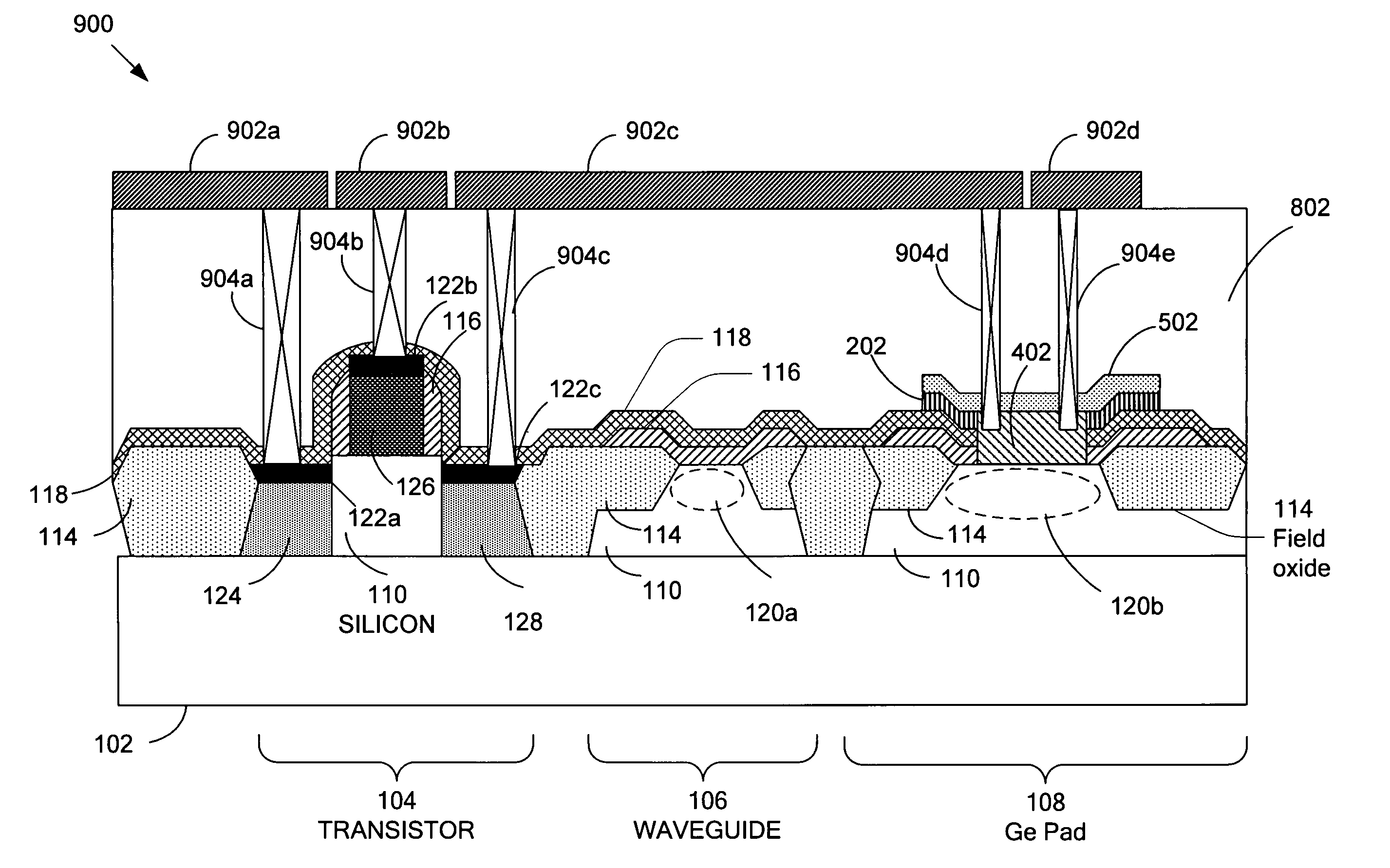
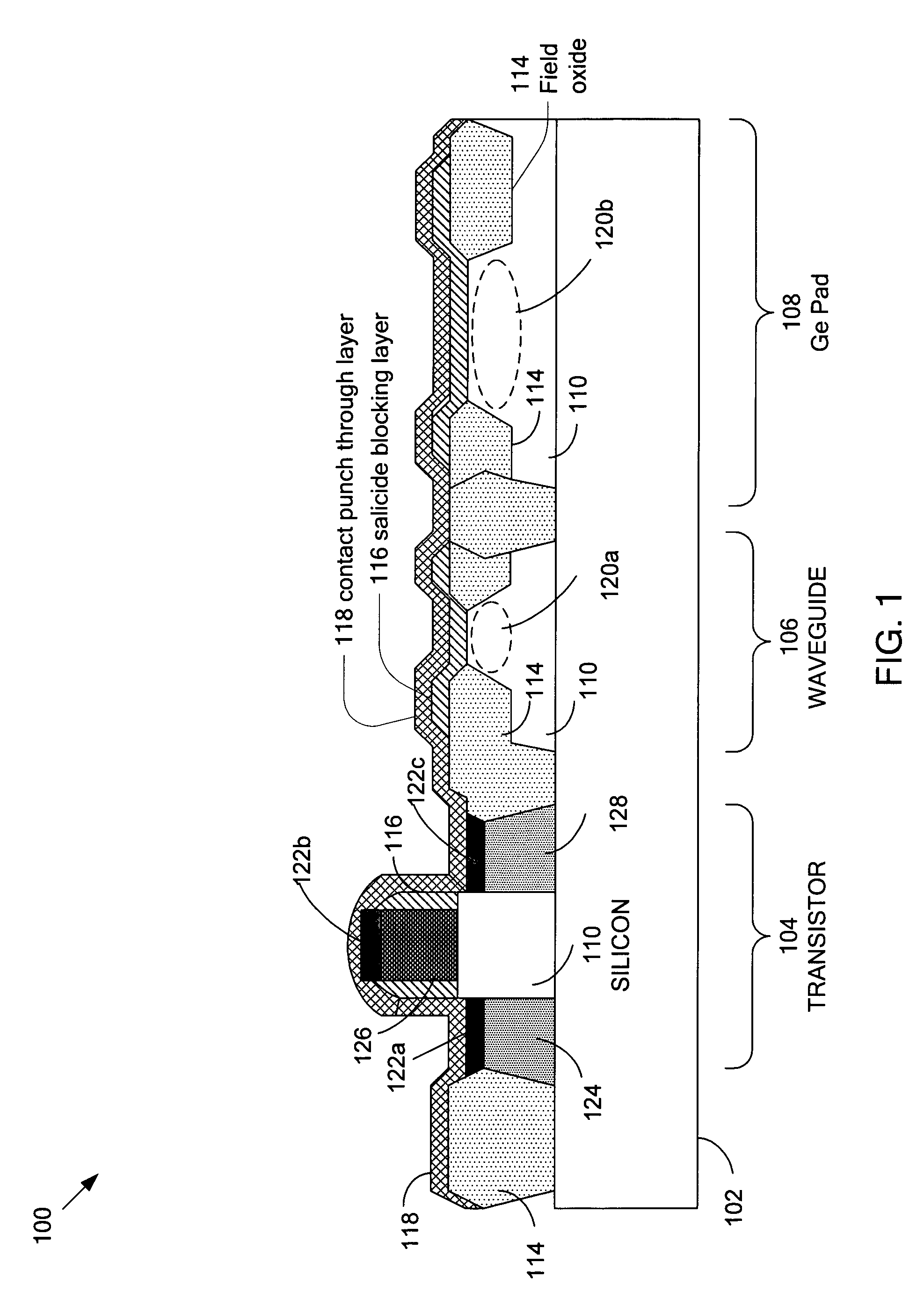
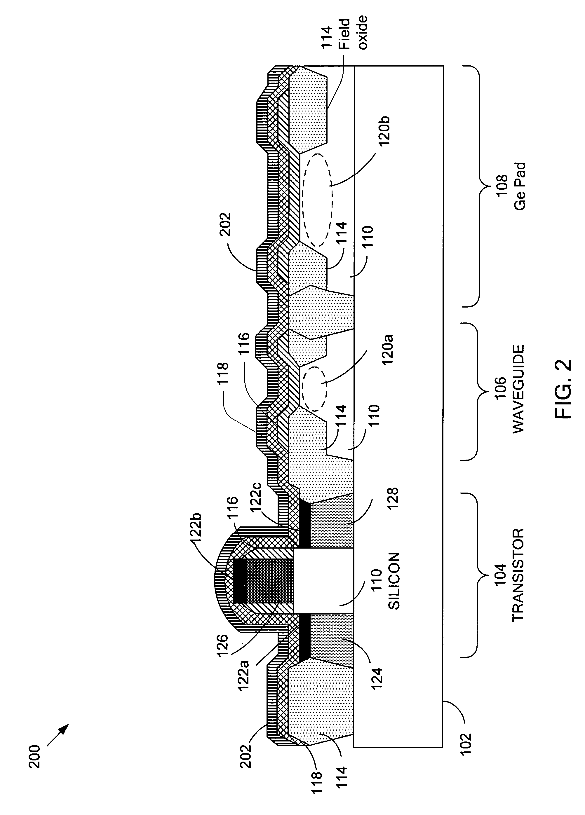
[0027]The present invention discloses an integration flow of germanium into a conventional CMOS process, with improvements in performing selective area growth, and implementing electrical contacts to the germanium, in a way that has minimal impact on the preexisting transistor devices. The present invention also provides methods to integrate the germanium without impacting the optical or electrical performance of these devices, except where intended, such as in a germanium photodetector, or germanium waveguide photodetector.

[0028]FIG. 1 is a schematic cross sectional diagram of an exemplary embodiment 100 of CMOS wafer, illustrating its layer structure at insertion point into the CMOS process in accordance with one embodiment of the present teachings. The embodiment 100 includes a substrate 102, preferably made of silicon, and three portions over the substrate 102; transistor 104, waveguide 106 and Ge pad 108. At this point in the process, the Ge pad references the location at which...


PUM


Abstract

The present invention discloses an integration flow of germanium into a conventional CMOS process, with improvements in performing selective area growth, and implementing electrical contacts to the germanium, in a way that has minimal impact on the preexisting transistor devices. The present invention also provides methods to integrate the germanium without impacting the optical or electrical performance of these devices, except where intended, such as in a germanium photodetector, or germanium waveguide photodetector.

Description

[0001]This application is a continuation-in-part of application Ser. No. 10 / 458,165, filed on Jun. 10, 2003, now U.S. Pat. No. 6,887,773, and claims the benefit of U.S. Provisional Application Ser. No. 60 / 645,808, filed on Jan. 21, 2005, entitled “Provisional disclosure on a process for integration of germanium into a CMOS fabrication process,” which are incorporated herein by their entirety.BACKGROUND INFORMATION[0002]1. Field of the Invention[0003]The invention relates generally to the field of chip manufacturing process, and more particularly to a process for integrating germanium into a CMOS fabrication process.[0004]2. Description of Related Art[0005]The convergence of silicon and optical fabrication processes presents an attractive manufacturing solution by leveraging the use of a standard CMOS (complementary metal-oxide semiconductor) manufacturing process. Integration of germanium (Ge) in a CMOS process has been desired for a number of reasons. Firstly, Ge has a smaller band...

Claims


Application Information

Patent Timeline
IPC IPC(8): H01L21/20
CPCH01L21/26506H01L21/76816H01L29/665H01L21/8238H01L21/823871H01L27/0617
Inventor GUNN, III, LAWRENCE C.CAPELLINI, GIOVANNIMASINI, GIANLORENZO
Owner CISCO TECH INC
Why Eureka
Try Eureka