

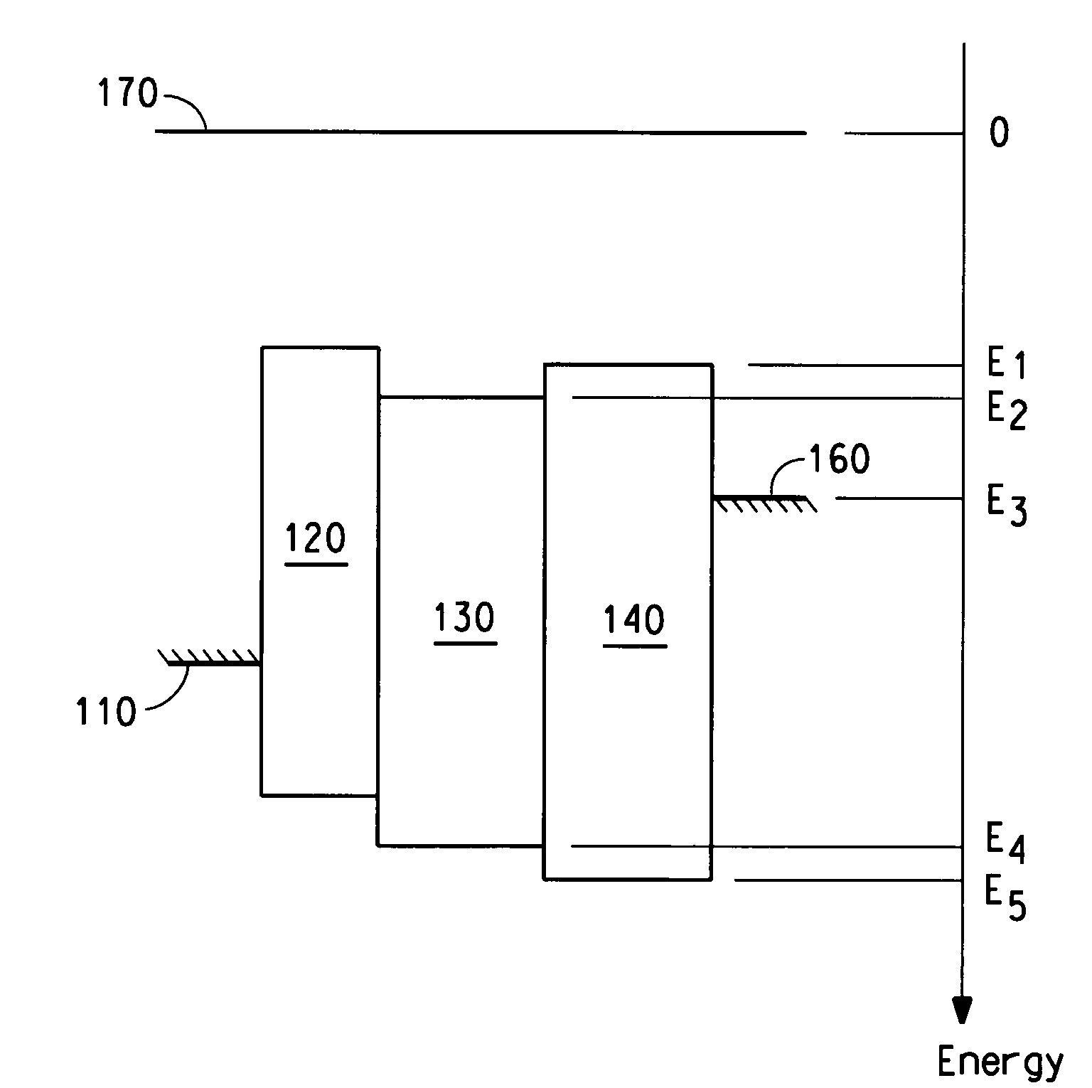
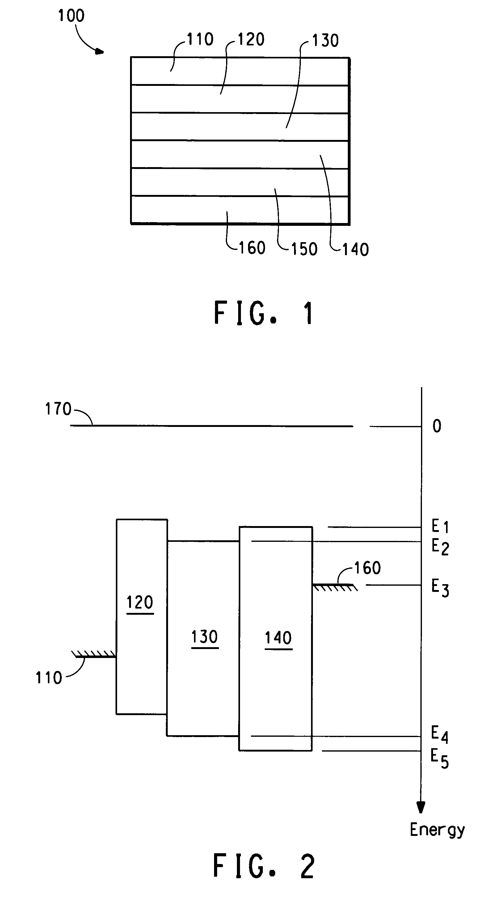
Electronic devices made with electron transport and/or anti-quenching layers
a technology of electron transport and electron transport layer, applied in the field of photoactive electronic devices, can solve the problems of insufficient use of large band gap exciton blockers, and achieve the effect of reducing both electron transfer quenching and energy transfer quenching of the photoactive layer
- Summary
- Abstract
- Description
- Claims
- Application Information
AI Technical Summary
Benefits of technology
Problems solved by technology
Method used
Image

Examples
examples
[0089]The following examples illustrate certain features and advantages of the present invention. They are intended to be illustrative of the invention, but not limiting. All percentages are by weight, unless otherwise indicated.
examples 1-17
[0090]These examples illustrate the preparation of some ET / AQ compositions.
example 1
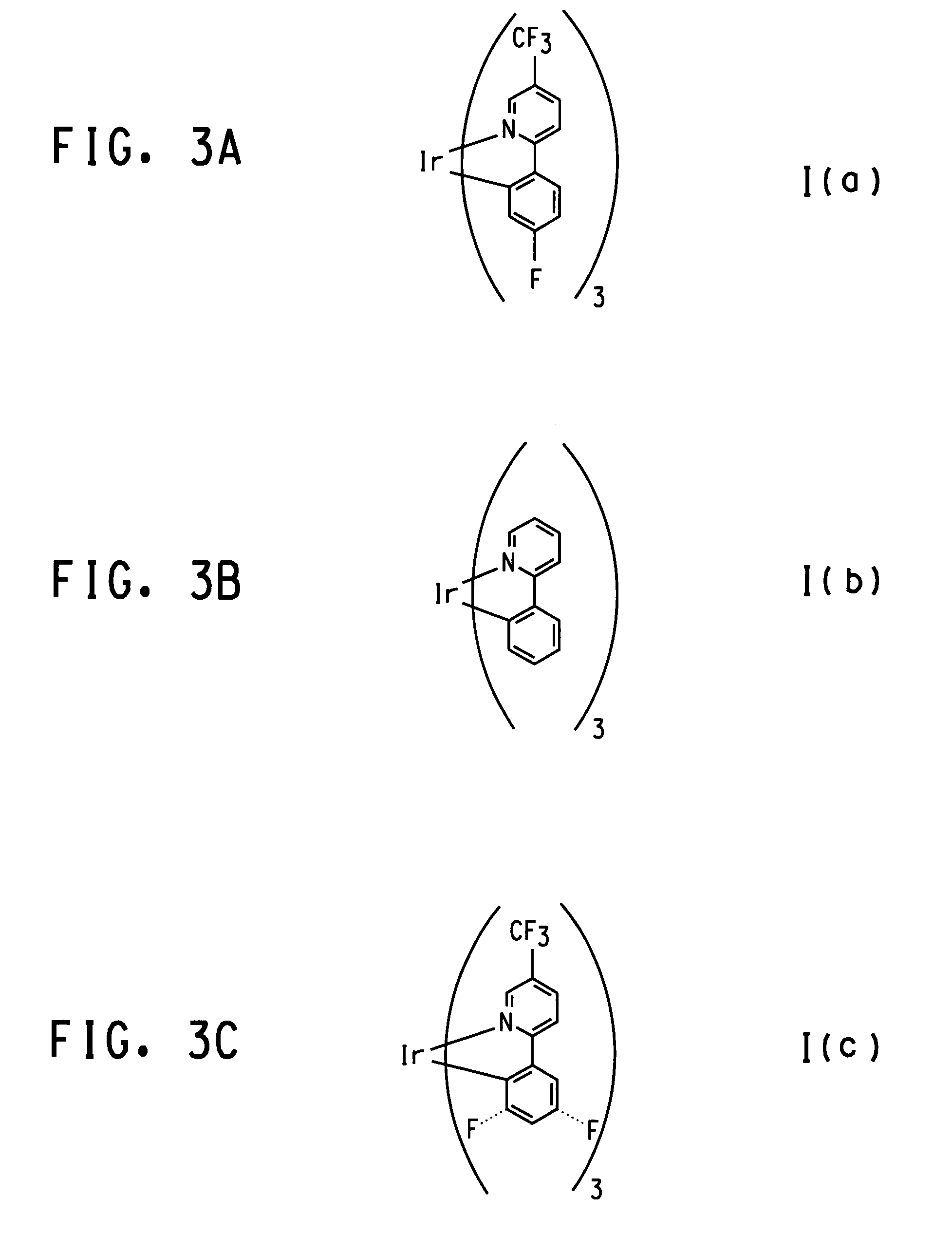
[0091]This example illustrates the preparation of Compound V(b) in FIG. 9.
[0092]A mixture of 3,4-diaminotoluene (28.78 g, 0.236 mol) and benzil (45 g, 0.214 mol) was refluxed in 738 ml chloroform with 2.16 ml trifluoroacetic acid for 3 hours. The mixture was washed 3 times with 10% HCl, brine, and dried over MgSO4, filtered, and then filtered through a silica bed with vacuum. The resultant solution was evaporated to dryness. Recrystalized 69 grams of crude product from 550 ml methanol. Filtered solids were dried in a vacuum oven at 50° C. for 1 hour to yield 55.56 g of dried solid. 78.8% yield
PUM
| Property | Measurement | Unit |
|---|---|---|
| energy barrier | aaaaa | aaaaa |
| temperature | aaaaa | aaaaa |
| temperature | aaaaa | aaaaa |
Abstract
Description
Claims
Application Information