System and method for high-order accurate device model approximation

Inactive Publication Date: 2007-09-04
CADENCE DESIGN SYST INC
View PDF8 Cites 3 Cited by
  • Summary
  • Abstract
  • Description
  • Claims
  • Application Information

AI Technical Summary

Benefits of technology

[0010]The present invention further includes a method for reducing memory usage during circuit simulations, comprising the steps of identifying one or more operating points; obtaining, for each of the one or more operat

Problems solved by technology

Modern analytical models such as bsim3 and bsim4 have become more and more complicated and expensive to evaluate in simulation.
As a result, model evaluation has become a bottle neck in the improvement of circuit simulation efficiency.
It is becoming more and more difficult to maintain some degree of smoothness in the approximated analytical model due to its complexity.
The problem associated with fixed stencil interpolations, however, is that for curves containing a C0 corner point (i.e. curves that are continuous but not differentiable at the comer point), fixed stencil interpolation of second or higher order accuracy will be necessarily oscillatory near the C0 co

Method used


Image

  • System and method for high-order accurate device model approximation
  • System and method for high-order accurate device model approximation
  • System and method for high-order accurate device model approximation

Examples


Example

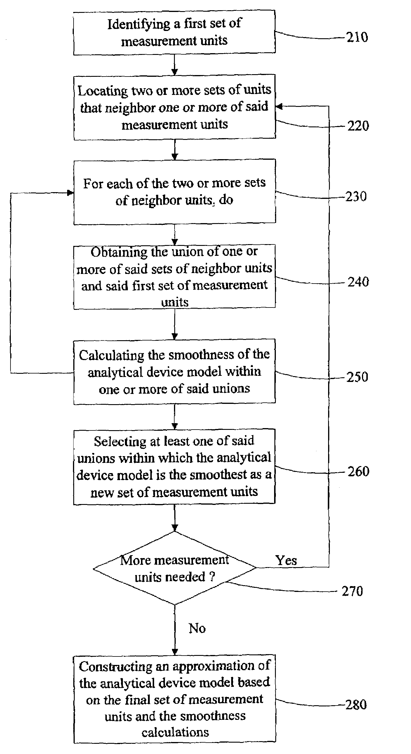
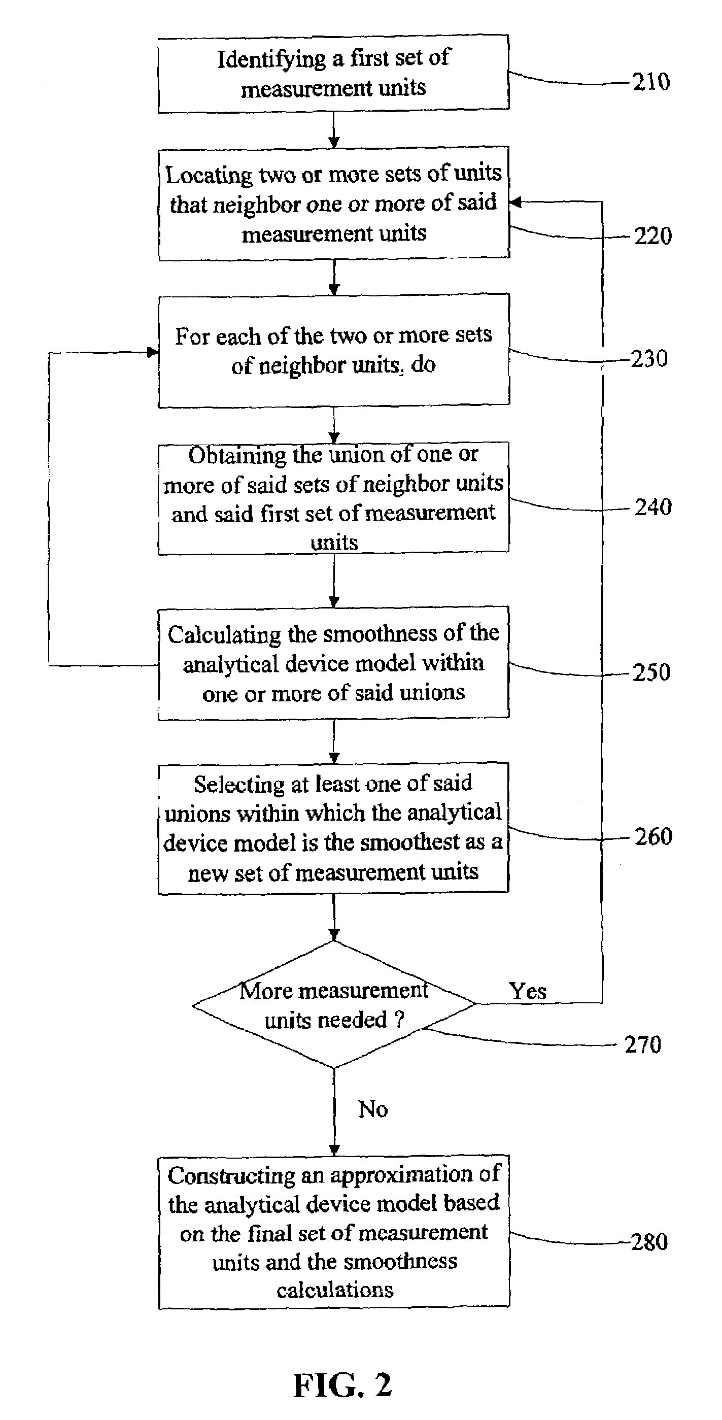
[0017]One preferred embodiment of the present invention uses dynamic stencils to obtain smooth and accurate approximations of analytical device models. A flow chart of this embodiment is depicted in FIG. 2. At step 210, a first set of measurement units is identified. Step 220 locates two or more sets of neighboring units that neighbor one or more of said measurement units. At steps 230–250, for each set of the two or more sets of neighboring units, the dynamic stencil scheme obtains the union of said each set and said first set of measurement units and calculates the smoothness of the analytical device model within the union. At step 260, the dynamic stencil scheme selects at least one of said unions within which the analytical device model is the smoothest as a new set of measurement units. Steps 220–260 are repeatedly iterated until the new set of units achieves the desired accuracy of the analytical device model. The approximated analytical device model is obtained at step 280 ba...


PUM


Abstract

An system and method are disclosed for efficiently approximating analytical circuit device models. A preferred embodiment includes a method for obtaining smooth and accurate approximations of analytical device models, comprising the steps of identifying a first set of measurement units; locating two or more sets of units that neighbor one or more of said measurement units; for each set of the two or more sets of neighbor units, obtaining the union of one or more of said sets of neighbor units and the first set of measurement units; calculating the smoothness of the analytical device model within one or more of said unions; and selecting at least one of said unions within which the analytical device model is the smoothest as the new set of measurement units.

Description

FIELD OF THE INVENTION[0001]The present invention relates generally to the field of device model approximation. More particularly, the present invention relates to an efficient system and method for approximating analytical circuit device models.BACKGROUND OF THE INVENTION[0002]Simulation is an indispensable verification step before committing an integrated circuit to an expensive manufacturing process. An important step in circuit simulation is model evaluation. Modern analytical models such as bsim3 and bsim4 have become more and more complicated and expensive to evaluate in simulation. The percentage of model evaluation time in circuit simulation can be as high as 70–80%. This number can grow to 90% if one includes simulation time spent in using all the individual device evaluations to generate the circuit equations. As a result, model evaluation has become a bottle neck in the improvement of circuit simulation efficiency.[0003]It is becoming more and more difficult to maintain s...

Claims


Application Information

Patent Timeline
IPC IPC(8): G06F17/50G06F17/10G06T17/20G06F17/17
CPCG06F17/17G06F17/5036G06F30/367
Inventor YANG, BAOLINMCGAUGHY, BRUCE W.
Owner CADENCE DESIGN SYST INC
Why Eureka
Try Eureka