Technique for operating a delay circuit

a delay circuit and delay technology, applied in the field of electronic circuits, can solve the problems of parasitic troublesome electronic circuits, inductors induced voltage fluctuations, etc., and achieve the effect of reducing inductive noise and inductive nois

Active Publication Date: 2007-09-11
RAMBUS INC
View PDF13 Cites 34 Cited by
  • Summary
  • Abstract
  • Description
  • Claims
  • Application Information

AI Technical Summary

Problems solved by technology

This phenomenon can be troublesome for electronic circuits that accommodate fast-switching operations.
Rapidly changing currents can induce voltage fluctuations (i.e., inductive noise) in parasitic inductors that are inherent in most circuits.
For example, a memory array employing a differential bi-directional bus may have inductive noise problems.
During a bus-turnaround between READ and WRITE operations, current ramp profiles on the memory array's power supply rails can induce large voltage fluctuations as well as ground bounce.
Such inductive noise problems can be exacerbated when a memory chip is packaged with inexpensive materials with large associated parasitic inductances.
Selection of the position of power and ground pins on the package can also affect inductive noise.
However, these solutions are typically useful only to the specific circuits for which they are designed.
There has not been a system-level solution that can reduce the effect of inductive noise regardless of the underlying physical circuits.

Method used


Image

  • Technique for operating a delay circuit
  • Technique for operating a delay circuit
  • Technique for operating a delay circuit

Examples


Embodiment Construction

)

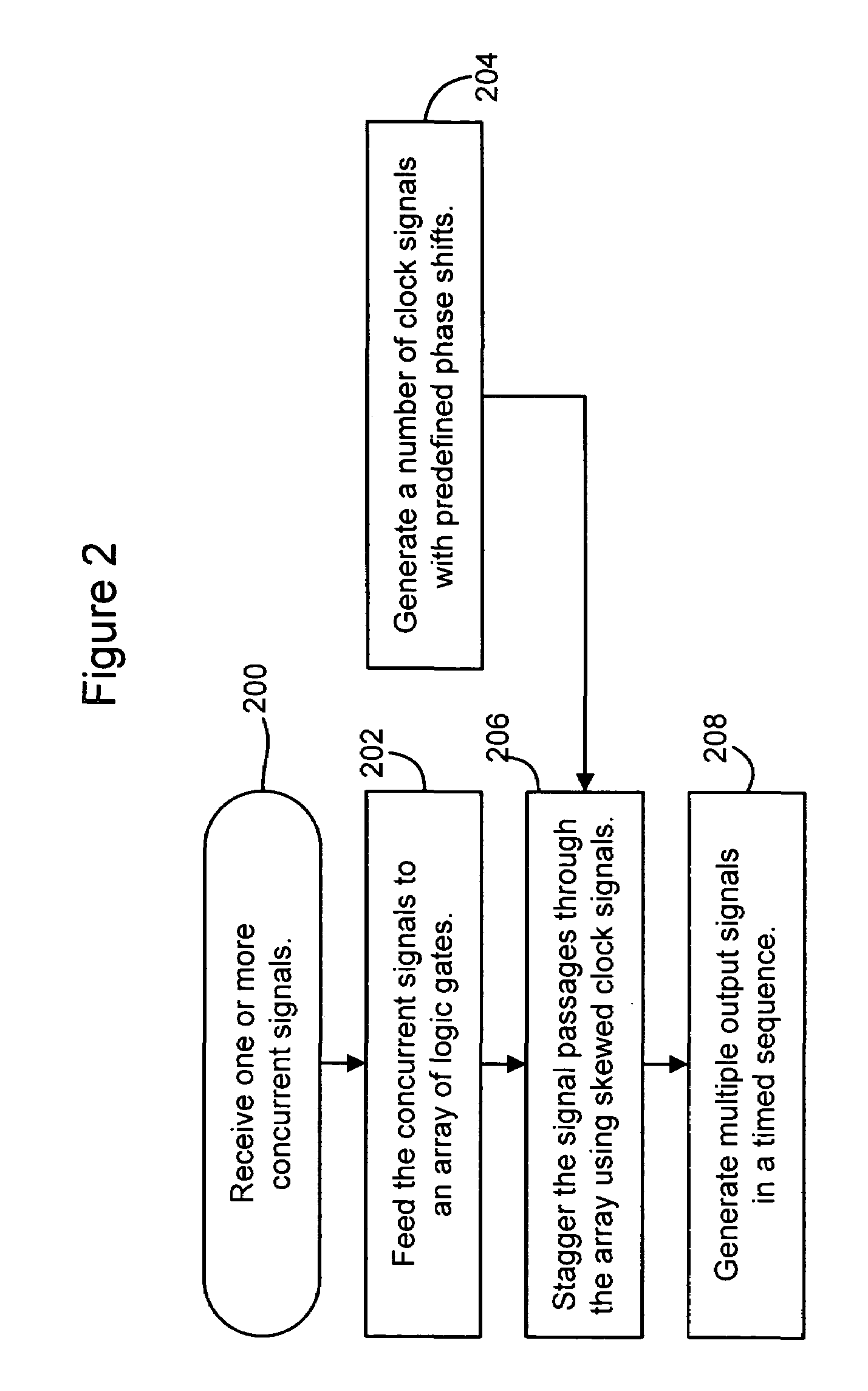
[0025]Referring to FIG. 2, there is shown a flow chart illustrating an exemplary method for operating a delay circuit in accordance with an embodiment of the present disclosure.

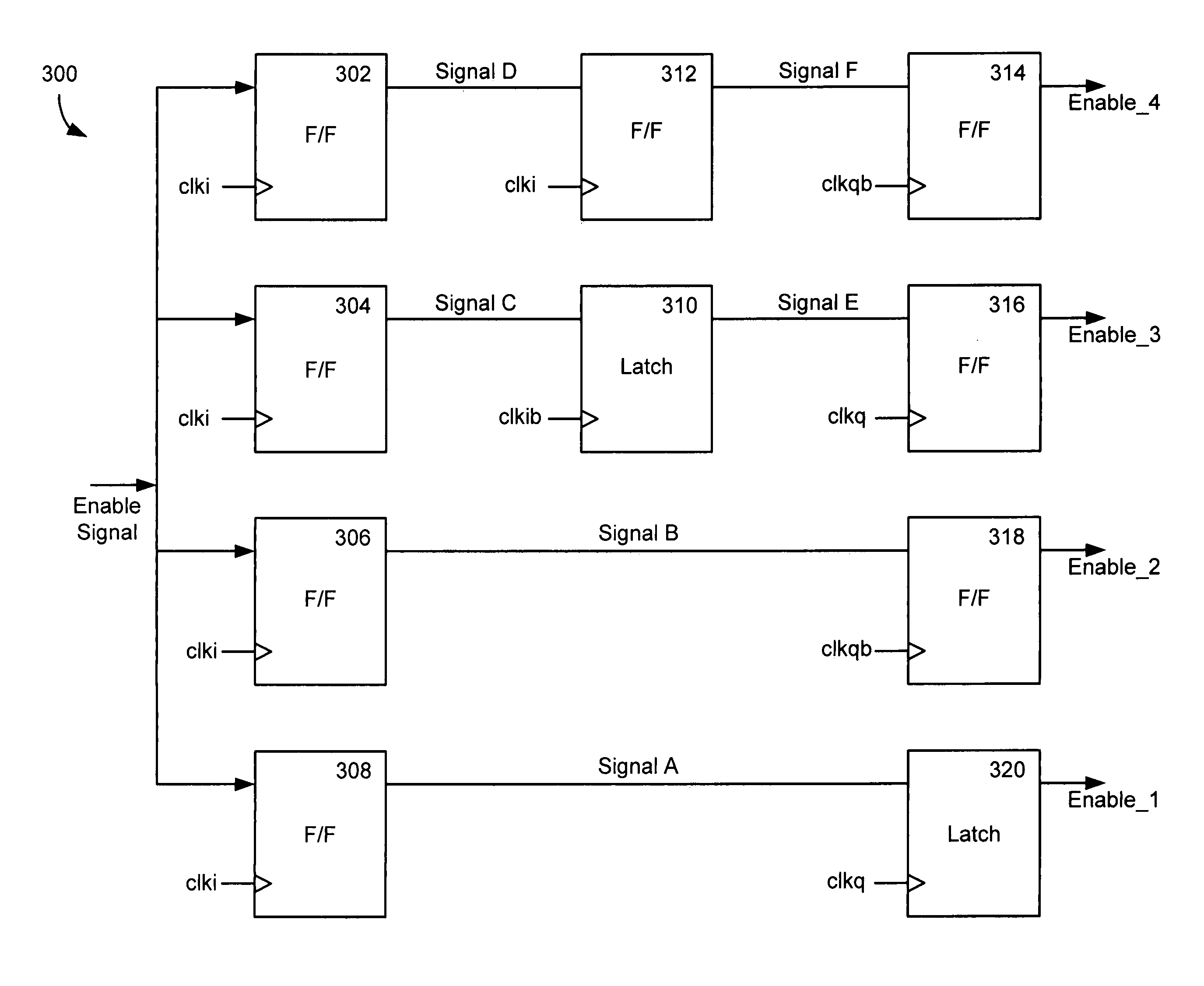
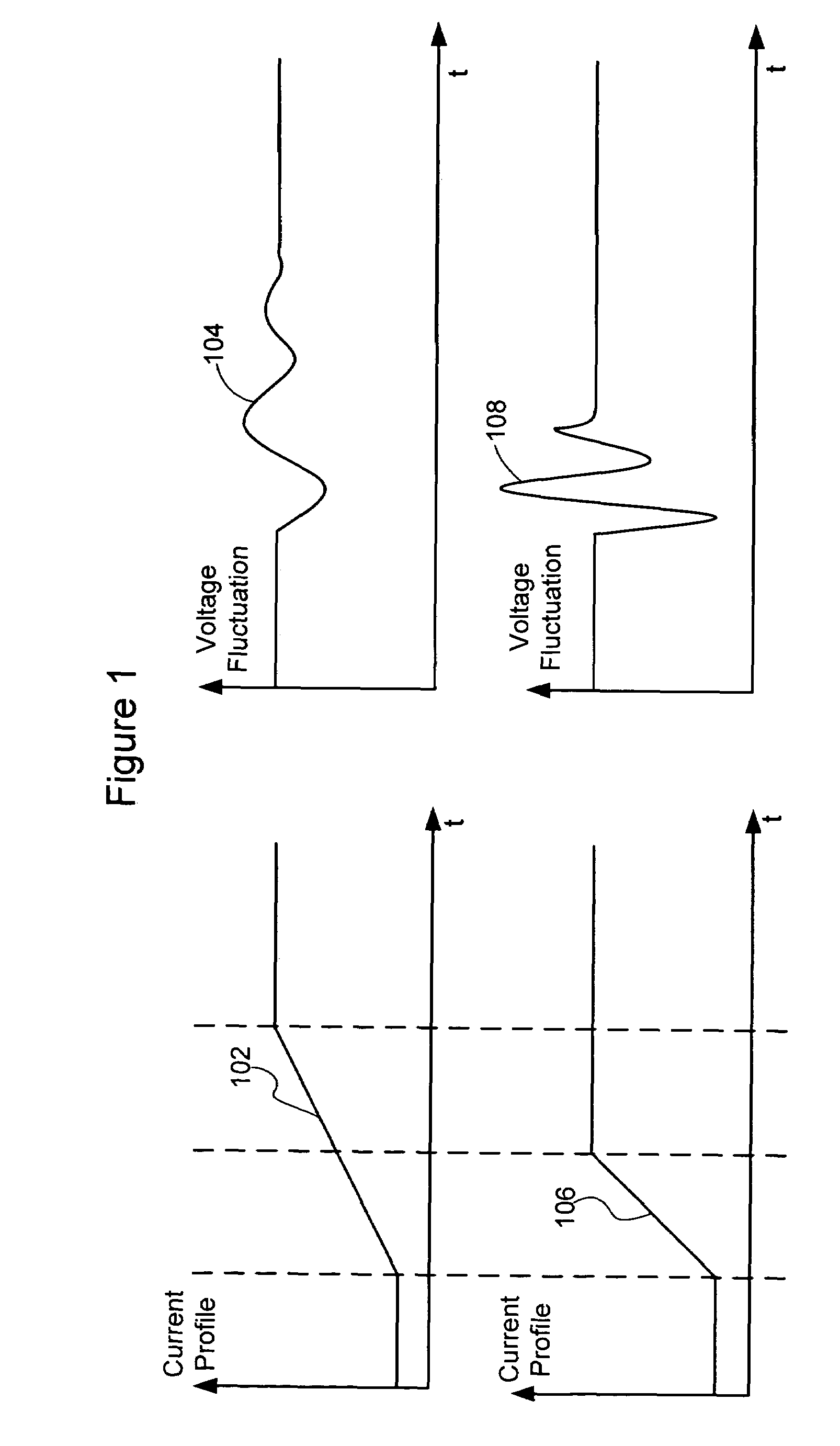
[0026]In step 200, one or more substantially concurrent signals may be received. The one or more concurrent signals may be digital control signals associated with a memory array. For example, an ENABLE signal may be provided for transmission to a number of transmit systems that are part of a DRAM's I / O subsystem. Without any control, the ENABLE signal would be sent to the transmit systems simultaneously, causing a rapid current ramp on the power rail. To avoid such a rapid change in current, it may be desirable to control the delivery of the ENABLE signal in a non-simultaneous manner.

[0027]In step 202, the one or more substantially concurrent signals may be fed to an array of logic gates. The array of logic gates may include flip-flops and latches arranged in such a topology that they provide a number of dat...


PUM


Abstract

A technique for operating a delay circuit is disclosed. In one particular exemplary embodiment, the technique may be realized by a delay circuit comprising a plurality of data paths. The delay circuit may receive a signal. The delay circuit may also stagger transmissions of the signal through the plurality of data paths. The delay circuit may additionally generate a plurality of signals based on the staggered transmissions. Each of the plurality of data paths in the delay circuit may comprise at least one of an inverter, a logic gate, a flip-flop, a latch, a register, or a resistor-capacitor (RC) delay element.

Description

FIELD OF THE DISCLOSURE[0001]The present disclosure relates generally to electronic circuits and, more particularly, to a technique for operating a delay circuit to reduce inductive noise.BACKGROUND OF THE DISCLOSURE[0002]It is well known that an inductor typically resists a change in the current flowing through it by generating a counteracting voltage drop. This phenomenon can be troublesome for electronic circuits that accommodate fast-switching operations. Rapidly changing currents can induce voltage fluctuations (i.e., inductive noise) in parasitic inductors that are inherent in most circuits. For example, a memory array employing a differential bi-directional bus may have inductive noise problems. During a bus-turnaround between READ and WRITE operations, current ramp profiles on the memory array's power supply rails can induce large voltage fluctuations as well as ground bounce. Such inductive noise problems can be exacerbated when a memory chip is packaged with inexpensive ma...

Claims


Application Information

Patent Timeline
Patent Type & Authority Patents(United States)
IPC IPC(8): H03H11/26H03K19/003
CPCH03K19/00346
Inventor FANG, WAYNERICHARDSON, WAYNE S.WONG, ANTHONY
Owner RAMBUS INC
Why Eureka
Try Eureka