Piezoelectric device mounted on integrated circuit chip

a technology of integrated circuit chip and piezoelectric device, which is applied in the direction of solid-state devices, generators/motors, semiconductor devices, etc., can solve the problems of low circuit density and large area consumed by plastic packages on the mounting surfa

Active Publication Date: 2007-09-18
ALFRED E MANN FOUND FOR SCI RES
View PDF20 Cites 23 Cited by
  • Summary
  • Abstract
  • Description
  • Claims
  • Application Information

AI Technical Summary

Problems solved by technology

The use of such packages results in a low circuit density as the ceramic or plastic package consumes relatively large areas of the mounting surface, particularly if a socket is used.

Method used


Image

  • Piezoelectric device mounted on integrated circuit chip
  • Piezoelectric device mounted on integrated circuit chip
  • Piezoelectric device mounted on integrated circuit chip

Examples


Embodiment Construction

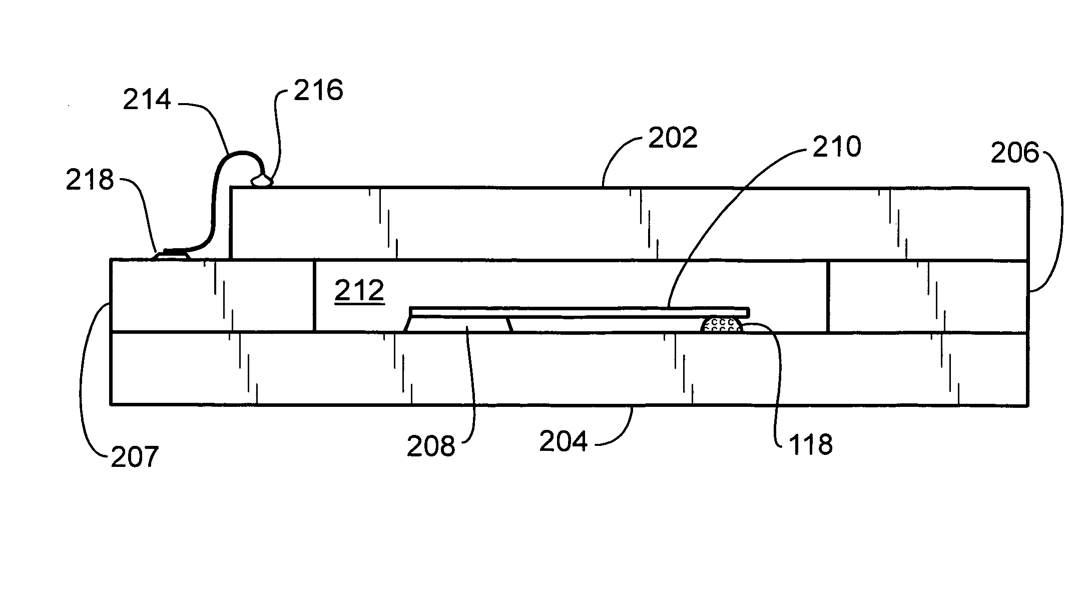
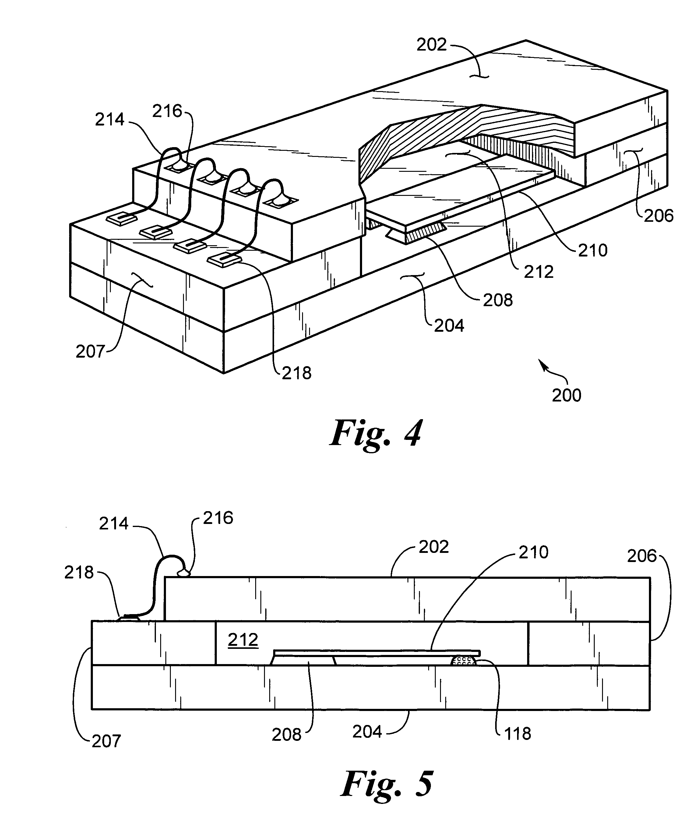
[0022]Size reduction can be achieved by eliminating the ceramic and glass box that the electromechanical resonator is normally packaged in, or by combining the oscillator integrated circuit (IC) and other appropriate circuit elements in one package. Size reduction is facilitated by having a method for mounting an electromechanical resonator directly on an IC chip. Small size offers a great benefit to electronic microdevices that are suitable for implantation in living tissue. One preferred application is the BION® device of Advanced Bionics, a Boston Scientific company, that is preferably less than 60 mm in axial length and less than 6 mm in lateral dimension or diameter, if a cylinder. Such devices are suitable for implantation by injection. U.S. Pat. Nos. 4,991,582; 5,193,539; 5,193,540; and 5,324,316 disclose such devices and are incorporated in their entirety herein by reference.

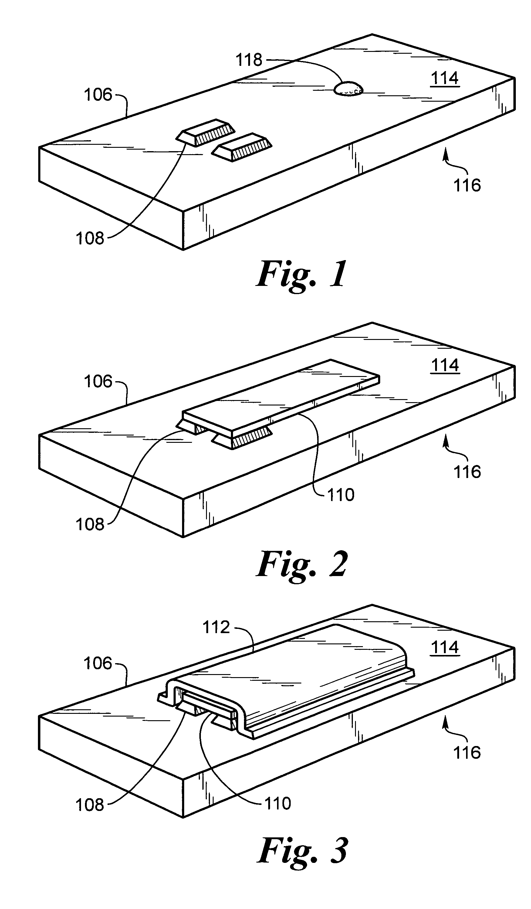
[0023]FIG. 1 provides a perspective view of a preferred embodiment of the electromechanical resonator...


PUM

PropertyMeasurementUnit
diameteraaaaaaaaaa
lengthaaaaaaaaaa
axial lengthaaaaaaaaaa

Abstract

An electronics filter circuit includes an electromechanical resonator that is mounted directly to the surface of a silicon integrated circuit, rather than being a surface mounted or leaded filter can on a circuit board. This filter circuit allows the integrated circuit electronic package to be significantly smaller than a conventional electromechanical resonator package. The electromechanical resonator may be protected during processing and during use with a protective cover that is made of a material such as titanium. The protective cover is attached to the integrated circuit chip.

Description

CROSS REFERENCE TO RELATED APPLICATION[0001]This application is a continuation-in-part of U.S. patent application Ser. No. 10 / 342,825, filed Jan. 15, 2003, now abandonedFIELD OF THE INVENTION[0002]This invention relates to high-density electronic modules, which incorporate more electronic capacity in a given space, or which reduce the space required for a given amount of electronic capacity, by placing the mechanical resonator directly on the integrated circuit chip. One of the primary uses of the present invention is to provide size reduction for integrated circuitry useful in implantable microstimulators and microsensors for implantation in living tissue.BACKGROUND OF THE INVENTION[0003]Most integrated circuits (ICs) and other miniature components such as oscillators, magnetic sensors, etc. are packaged in plastic or ceramic packages with solder pads or with extending metal leads for soldering to a printed circuit board or for insertion into a socket. Piezoelectric devices are com...

Claims


Application Information

Patent Timeline
Patent Type & Authority Patents(United States)
IPC IPC(8): H01L41/08H03H3/02H03H9/10
CPCH03H9/1021Y10T29/4908Y10T29/49007Y10T29/49005H01L2224/48227H01L2224/48465H01L2924/00H03H9/54H05K13/04
Inventor BYERS, CHARLES L.SCHULMAN, JOSEPH H.SCHNITTGRUND, GARY D.
Owner ALFRED E MANN FOUND FOR SCI RES
Why Eureka
Try Eureka