Electro-optical device and driving device thereof

a technology of optical devices and driving devices, applied in the direction of static indicating devices, identification means, instruments, etc., can solve the problems of difficult homogenization of electrical characteristics of pixel circuits for all pixels, crystalline defects may be generated, and deviations in characteristic during recrystallization can be easily generated, etc., to achieve excellent display quality, excellent display quality, and more accuracy

Active Publication Date: 2007-09-25
ELEMENT CAPITAL COMMERCIAL CO PTE LTD
View PDF32 Cites 109 Cited by
  • Summary
  • Abstract
  • Description
  • Claims
  • Application Information

AI Technical Summary

Benefits of technology

[0047]According to the invention, since the electro-optical elements manufactured through a conventional manufacturing method can be driven by means of a driving circuit comprising mono-channel TFTs such as α-TFTs, it is possible to realize a large-size electro-optical device, which was not possible conventionally. Specifically, when the invention can be applied to an organic EL display device, it is possible to obtain an active substrate capable of realizing a large-screen display, which is very thin and has excellent display quality. When different kinds of periodic control lines are required in the scanning line direction every pixel driving circuit in order to adjust a moving picture having a sharp profile or a display brightness with a wide range, the pixel driving circuits can be controlled by combination of the scanning lines without increase in the number of connection terminals, so that it is possible to realize a display having excellent display quality with more accuracy.

Problems solved by technology

However, in the low-temperature polysilicon TFT, deviation in characteristic during recrystallization thereof can be easily generated, and crystalline defects may be generated.
For this reason, in a display device employing thin film transistors formed out of low-temperature polysilicon TFTs, it is extremely difficult to homogenize the electrical characteristics of the pixel circuits for all pixels.
Specifically, since possibility that deviation in characteristics of the pixel circuits can be generated is further increased with increase in the number of pixels for increase in accuracy of display images or increase in screen size, a problem of decrease in display quality become more serious.
Furthermore, because of restriction of a laser anneal apparatus for performing recrystallization, it is difficult to increase a substrate size and thus enhance productivity as in amorphous TFTs (α-TFTs).
On the other hand, the α-TFTs have relatively small deviation in characteristics of transistors and have actual achievement of mass production through increase of a substrate size in LCD performing an alternating current driving, but since a threshold voltage is shifted by normally and continuously applying the gate voltage in one way, current values are changed and the luminance is lowered, thereby having a bad influence on display quality.
Furthermore, since the α-TFT has a small mobility, the current capable of performing the drive thereof with a fast response is restricted, and only the TFTs of n-channel are put to practical use.
Furthermore, due to restriction of the organic EL manufacturing technologies resulting from materials to be used, the conventional organic EL elements could not help having a structure that a TFT substrate side is used as a pixel electrode (anode) side and a surface side of the elements is used as a common electrode (cathode).

Method used


Image

  • Electro-optical device and driving device thereof
  • Electro-optical device and driving device thereof
  • Electro-optical device and driving device thereof

Examples


first embodiment

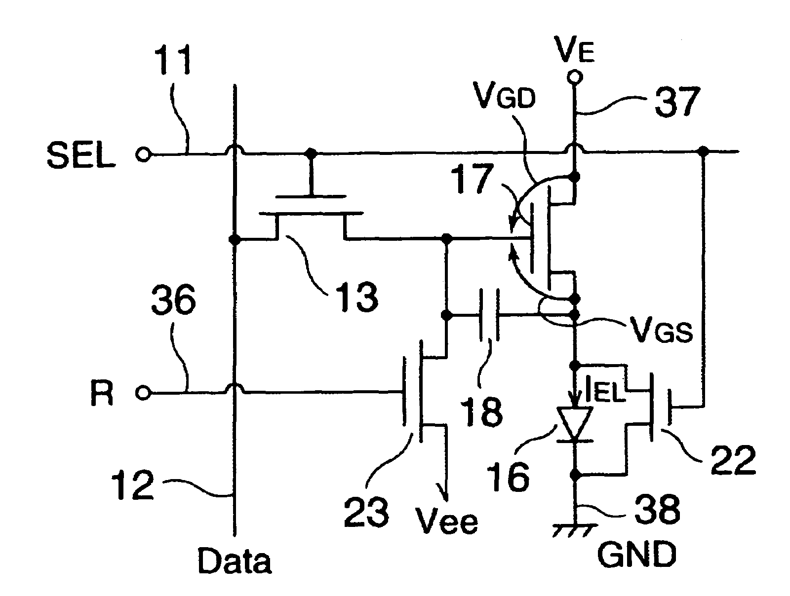
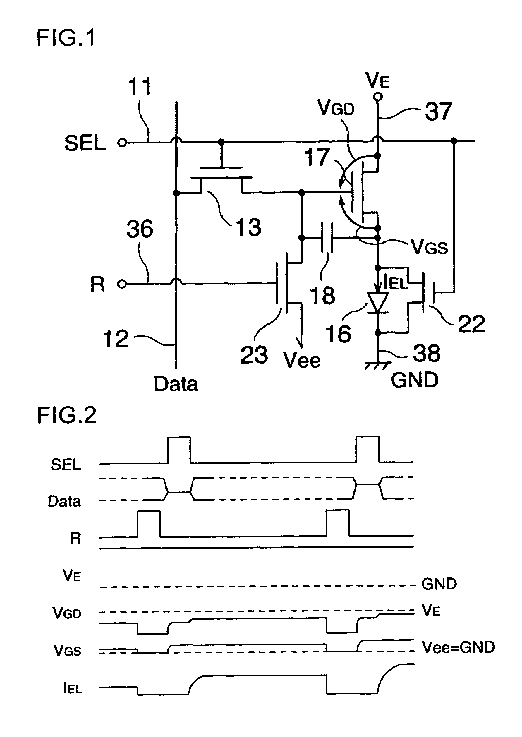
[0062]In the display pixel circuit shown in FIG. 1 which is the first embodiment, each display pixel PX can include an organic EL element 16, a driving transistor 17 which is an n-channel thin film transistor (TFT) connected in series to the organic EL element 16 between a pair of first and second power terminals VE and a ground power terminal GND, a storage capacitor 18 for holding the gate voltage of the driving transistor 17, an n-channel electrical conduction transistor 22 for allowing terminals of the organic EL element 16 to have substantially the same potential, a pixel selecting switch 13 for selectively applying an image signal from the corresponding data line 12 to the gate of the driving transistor 17, and a reset transistor 23 for initializing the gate potential of the driving transistor 17 into a predetermined potential Vee.

[0063]The power terminal VE is set to, for example, a predetermined potential of +28 V, and the ground power terminal GND is set to a potential of, ...

second embodiment

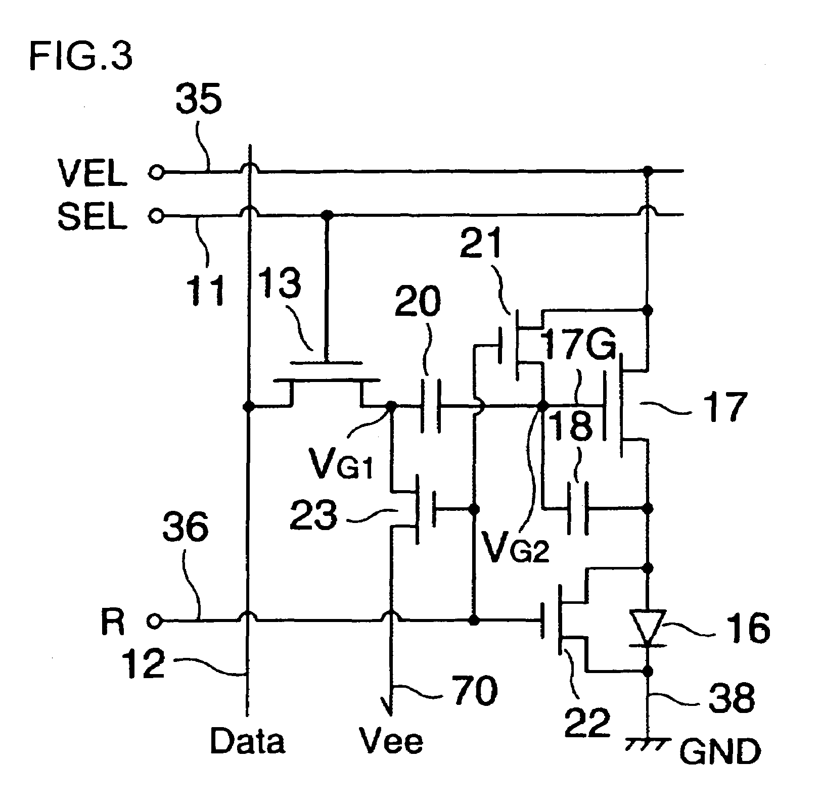
[0070]FIG. 3 shows a display pixel circuit according to the invention. A display pixel PX in the drawing can include a threshold voltage compensating circuit for the driving transistor 17, the threshold voltage compensating circuit including a kick capacitor 20 connected in series between the pixel selecting switch 13 and the gate electrode of the driving transistor 17, a bias transistor 21 connected between the gate electrode and the drain electrode of the driving transistor 17, the storage capacitor 18 connected between the gate electrode and the source electrode of the driving transistor 17, the electrical conduction transistor 22 for electrically connecting the pixel electrode and the common electrode (cathode) of an organic EL element, and the reset transistor 23 connected between a connection point of the pixel selecting switch 13 and the kick capacitor 20 and a power source Vee.

[0071]The respective transistors in the display pixel circuit are formed as an n-channel TFT, the p...


PUM


Abstract

The invention provides an electro-optical device having circuits for driving electro-optical elements, such as organic EL elements, and a driving device, which can employ driving elements having low driving ability, such as α-TFTs. By providing a charge storage capacitor between the source electrode and the gate electrode of a driving transistor which is between power sources, the electro-optical device can allow the driving transistor to control a driving current, even when an electro-optical element is connected to the source side of the driving transistor. In addition, driving data can be stored in the charge storage capacitor by applying a predetermined voltage to the source electrode of the driving transistor.

Description

BACKGROUND OF THE INVENTION[0001]1. Field of Invention[0002]The invention relates to an electro-optical device for performing display in information instruments such as televisions or computers. More specifically, the invention relates to a driving device for driving electro-optical elements such as organic electroluminescent elements.[0003]2. Description of Related Art[0004]In recent, since organic EL display devices have features as light weight, small thickness, high brightness, and wide viewing angle, the organic EL display devices had been paid attention to as monitor displays of portable information instruments, such as mobile phones. A typical active matrix organic EL display device has a construction that images are displayed through a plurality of display pixels arranged in a matrix. In the display pixels, a pixel circuit can be provided every pixel that is a minimum unit for display. The pixel circuits are circuits for controlling currents or voltages to be supplied to ele...

Claims


Application Information

Patent Timeline
Patent Type & Authority Patents(United States)
IPC IPC(8): G09G3/30G09F9/30G09G3/20H01L51/50G09G3/32G09G5/00H05B33/14
CPCG09G3/3233G09G3/3241G09G2300/0417G09G2300/043G09G2300/0819G09G2300/0842G09G2300/0852G09G2300/0861G09G2310/0251G09G2310/0254G09G2310/0256G09G2320/0261G09G2320/043B44C5/04B44C5/06B44C3/12B44C1/28
Inventor IMAMURA, YOICHIKASAI, TOSHIYUKIOZAWA, TOKURO
Owner ELEMENT CAPITAL COMMERCIAL CO PTE LTD
Why Eureka
Try Eureka