
Memory module and method for operating a memory module in a data memory system

Inactive Publication Date: 2007-09-25
POLARIS INNOVATIONS
View PDF6 Cites 26 Cited by
  • Summary
  • Abstract
  • Description
  • Claims
  • Application Information

AI Technical Summary

Benefits of technology

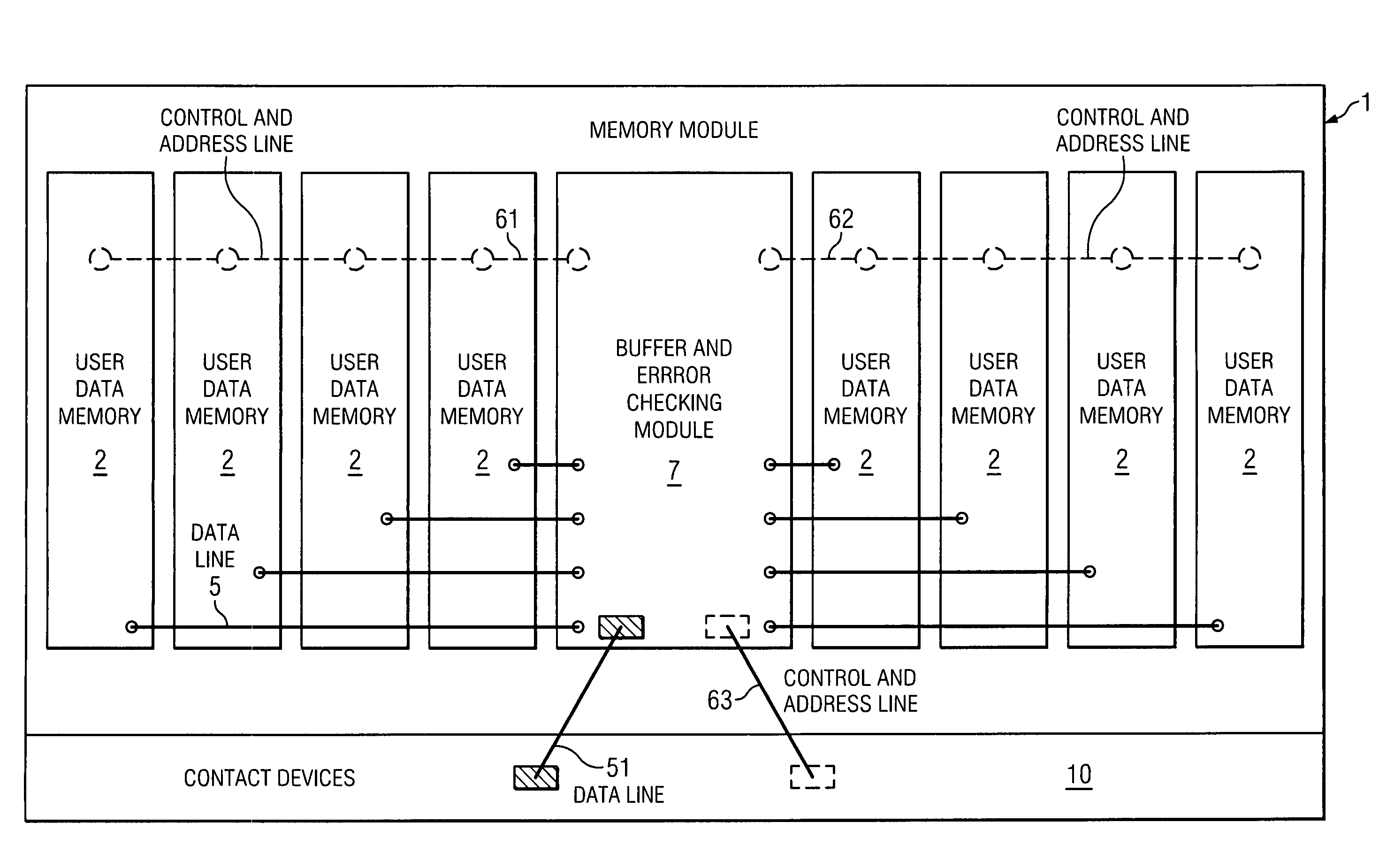
[0033]The memory module according to the invention for incorporation into a data memory system thus has at least one buffer and error checking module, which integrates in each case a buffer device and a data memory device for storing redundancy data within a common device housing.
[0049]According to a further preferred embodiment of the memory module according to the invention, the memory module has a possibility for signaling a data error. A memory module or a data memory device with accumulated error results can advantageously be identified through an evaluation of the data error in a higher processing plane of the data memory system. Repeatedly defective data memory areas can thus be masked out. The accompanying minimization of the number of error results further increases the performance of the data memory system.
[0033]The memory module according to the invention for incorporation into a data memory system thus has at least one buffer and error checking module, which integrates in each case a buffer device and a data memory device for storing redundancy data within a common device housing.

Problems solved by technology

An error event is present in this case if the user data transferred back to the memory checking module deviate from the user data originally transferred from the memory checking module to one of the data memory devices.
An error event is based on a transfer error, a defective memory cell in the data memory device or on a change in the data content of a memory cell brought about by ambient influences.
In the case of a defective addressing line within the data memory device, a usually undetectable or uncorrectable multiple error is converted into a number of generally correctable single errors.
However, a combination of an error correction concept with a buffer / redriver concept realized using conventional means also leads to disadvantages.
Thus, the high space requirement for the buffer / redriver modules and the error data memory makes it extraordinarily difficult to suitably form signal lines (routing) on memory modules whose dimensions are standardized according to JEDEC (joint electronic device engineering council).
Further disadvantages of simply combining error correction concepts on the one hand, and buffer / redriver concepts, on the other hand, occur with different weighting depending on a data bus width of the data memory devices provided on the memory module.
Since customary error correction concepts only utilize 8 bits, however, a data memory of the order of magnitude of an eighth of the entire memory capacity of the memory module disadvantageously remains unutilized.
A slot for the error data memory device is formed in the same way on the memory modules without error correction, but remains unpopulated.
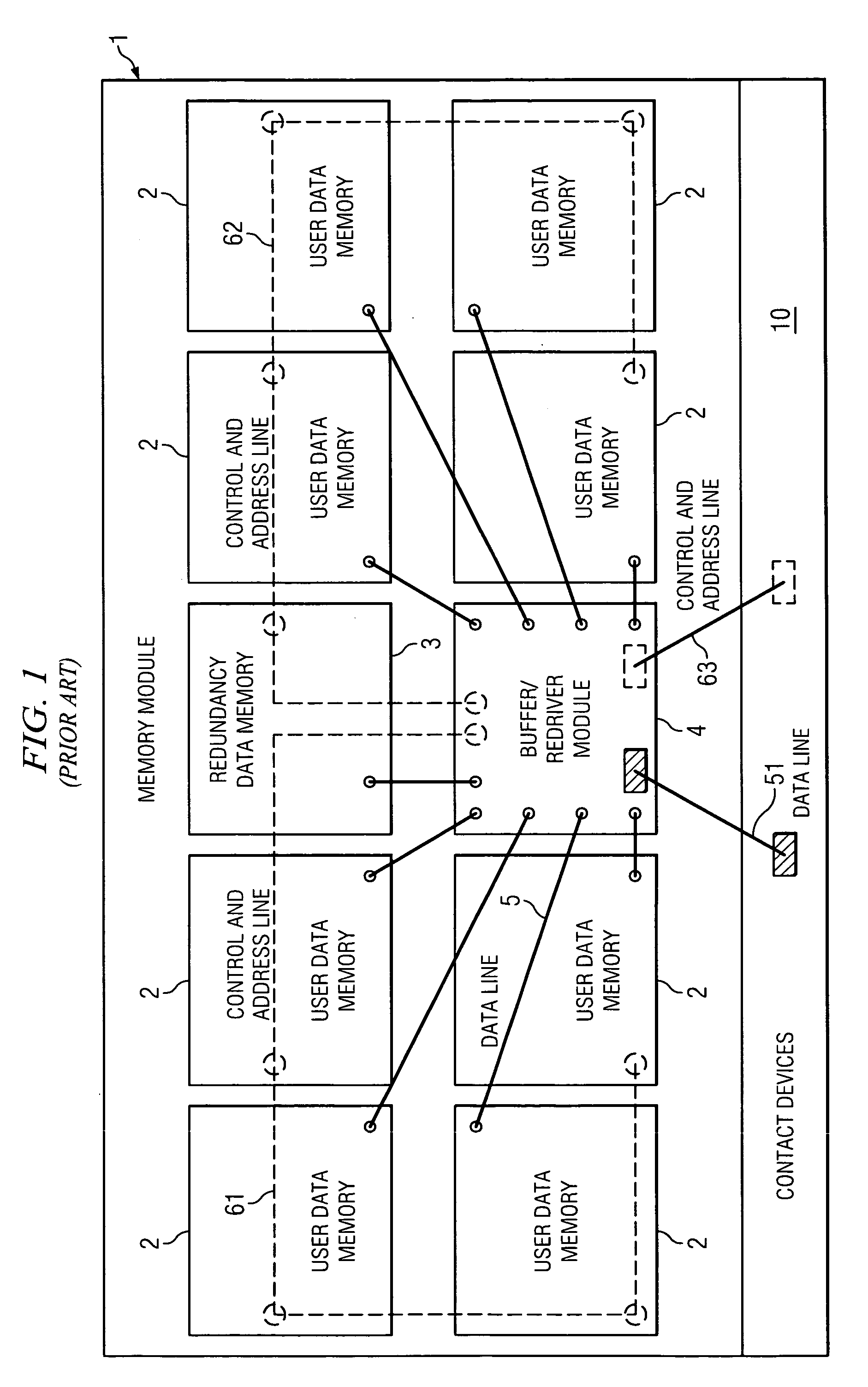
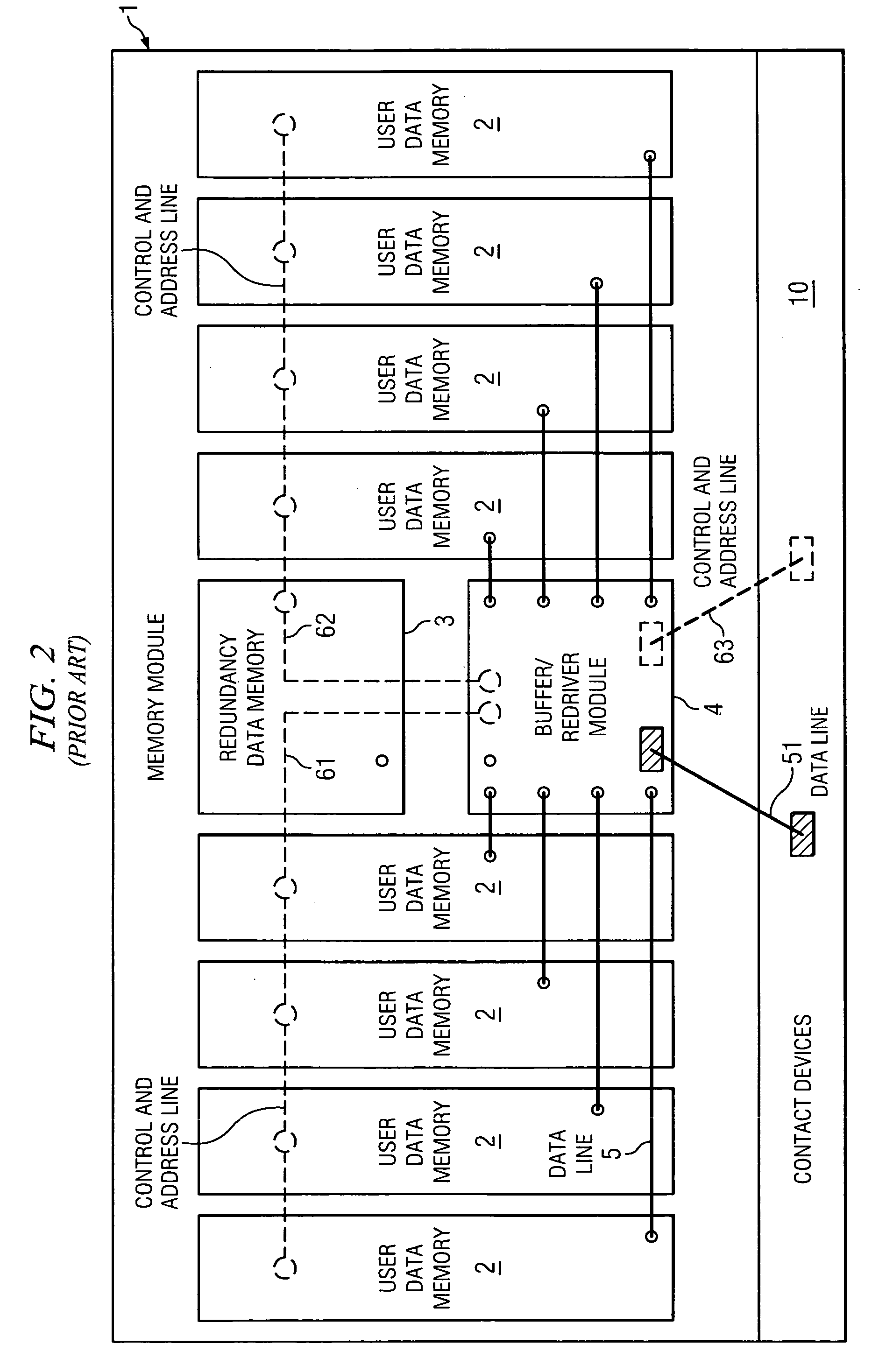
In a disadvantageous manner, however, no topology for the embodiment of the signal lines between the buffer / redriver module and the data memory devices then permits a symmetrical configuration of the in total nine slots for data memory devices on the memory module.
This leads to an asymmetrical formation of the data signal lines and the optimization of the timing of the data signals for the two configurations of the memory module with and without error correction is made more difficult.
However, this leads to an undesirable limitation of the data transfer rate and thus of the performance of the data memory system.
The space requirement of the memory cells in a semiconductor substrate of the data memory devices results in a comparatively large device size of the data memory devices used therefor.
The arrangement of additional buffer / redriver modules and of an additional error data memory device is not possible in these cases for space reasons.
Furthermore, it can be recognized that a routing of the data signal lines 5 is made considerably more difficult by the high population density of the memory module 1.

Method used


Image

  • Memory module and method for operating a memory module in a data memory system
  • Memory module and method for operating a memory module in a data memory system
  • Memory module and method for operating a memory module in a data memory system

Examples


Embodiment Construction

[0028]The following is a list of reference symbols used herein.

[0029]

 1Memory module10Contact devices 2Data memory device for user data 3Data memory device for redundancy data 4, 4′Buffer / redriver module 5Data lines internal51Data lines external61, 61′Control and address lines internal62, 62′Control and address lines internal63Control and address lines external 7, 7′Buffer and error checking module

[0030]FIG. 3 illustrates a memory module according to the invention. The routing of data signal lines 5 between the buffer and error checking module 7, which, according to the invention, integrates a buffer / redriver functionality and an error data memory in a common device housing, and the remaining DRAMs 2 for storing the user data is significantly simplified just by the omission of connections to the DRAM 3 for error data storage of FIG. 1 or 2. The same capacitive load is present on each branch 61, 62 of the internal control and address bus. In this case, the capacitive load is independ...


PUM


Abstract

Memory modules based on DDR-DRAMs are provided with a buffer and error checking module, which integrates an error data memory and a buffer / redriver functionality for conditioning data signals that are transferred to the memory module and output from the memory module and is suitable for the correction of user data stored erroneously in the DDR-DRAMs. The buffer and error checking module enables the integration of both error correction and buffer / redriver functionality on memory modules within the restricted memory module dimensions in accordance with definitive industry standards, simplified or improved routing of data lines and of control and address lines and also, by virtue of a reduction of erroneously transferred data to the data memory system, an increased real data transfer rate.

Description

TECHNICAL FIELD[0001]The invention relates to a memory module for operation in a data memory system.BACKGROUND[0002]Modular data memory systems usually have a system board with a plurality of slots for memory modules. The slots are occupied by memory modules in each case depending on the requirements made of the data memory system or on an expansion level of the data memory system.[0003]One example of a data memory system with a modular concept is a computer system (PC, workstation, server) with variable main memory in which slots for memory modules in the form of plug-in sockets are provided on a system board. The memory modules of modular data memory systems are generally present in the form of DIMMs (dual inline memory modules), whose mechanical and electrical interfaces to the system board are subject to industry standards.[0004]In order to increase the performance of such data memory systems, efforts are generally made to increase a clock or data transfer rate. Thus, data trans...

Claims


Application Information

Patent Timeline
IPC IPC(8): G11C29/00G11C7/10
CPCG11C7/1006G11C7/1066
Inventor RUCKERBAUER, HERMANNBRAUN, GEORG
Owner POLARIS INNOVATIONS
Learn More