Microfluidic devices with porous membranes for molecular sieving, metering, and separations

a microfluidic device and porous membrane technology, applied in the direction of fluid speed measurement, burettes/pipettes, ultrafiltration, etc., can solve the problems of increasing contamination risks, limiting the range of functions that may be accomplished by a single device or a combination of devices, and current microfluidic systems that do not adequately integrate a size-separating filter into a microfluidic chip

Active Publication Date: 2007-10-09
INTEL CORP
View PDF34 Cites 89 Cited by
  • Summary
  • Abstract
  • Description
  • Claims
  • Application Information

AI Technical Summary

Problems solved by technology

While the applications of such microfluidic devices may be virtually boundless, the integration of some microscale components into microfluidic systems has been technically difficult, thereby limiting the range of functions that may be accomplished by a single device or combination of devices.
In particular, current microfluidic systems have not adequately integrated a size-separating (or excluding) filter into a microfluidic chip.
As such, separations may generally be carried out in external packed porous media or polymer-based nanopore membranes, thereby increasing contamination risks and introducing additional complexity and manual interaction into the performance of an analysis or other technique.

Method used


Image

  • Microfluidic devices with porous membranes for molecular sieving, metering, and separations
  • Microfluidic devices with porous membranes for molecular sieving, metering, and separations
  • Microfluidic devices with porous membranes for molecular sieving, metering, and separations

Examples


Embodiment Construction

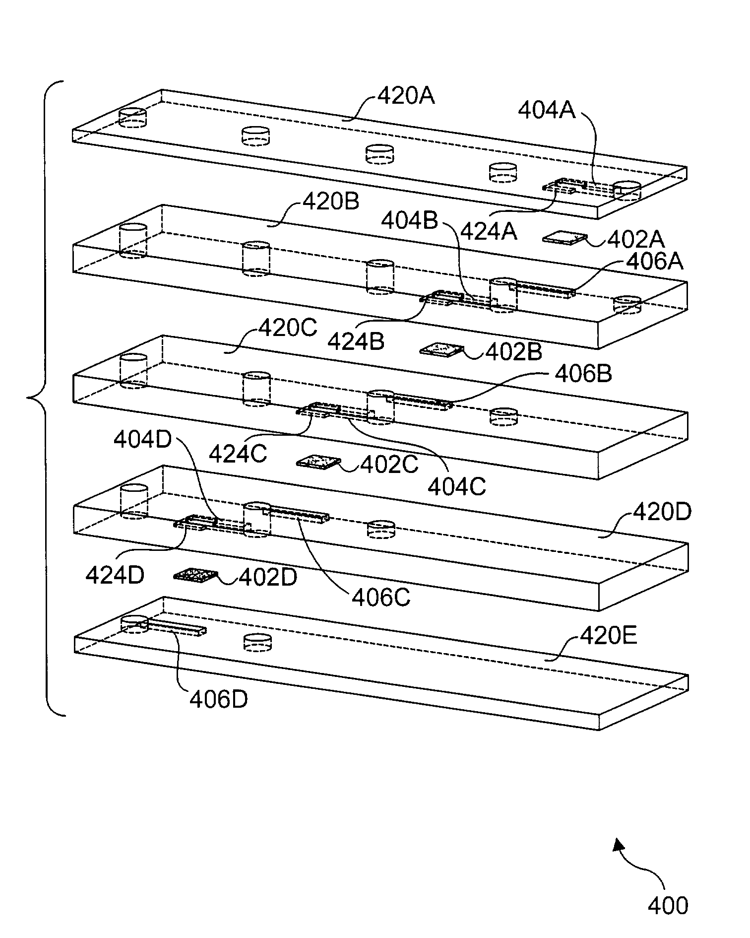
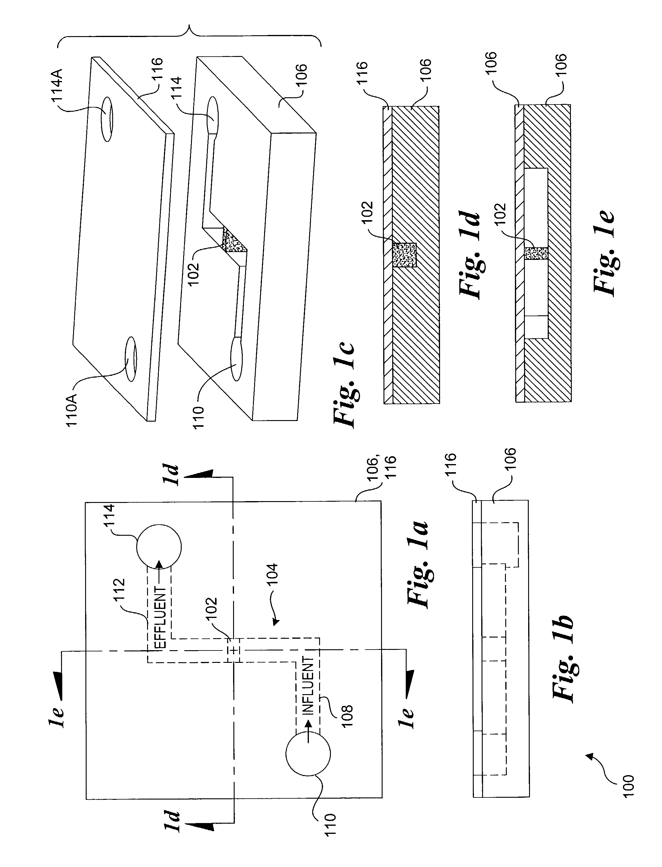
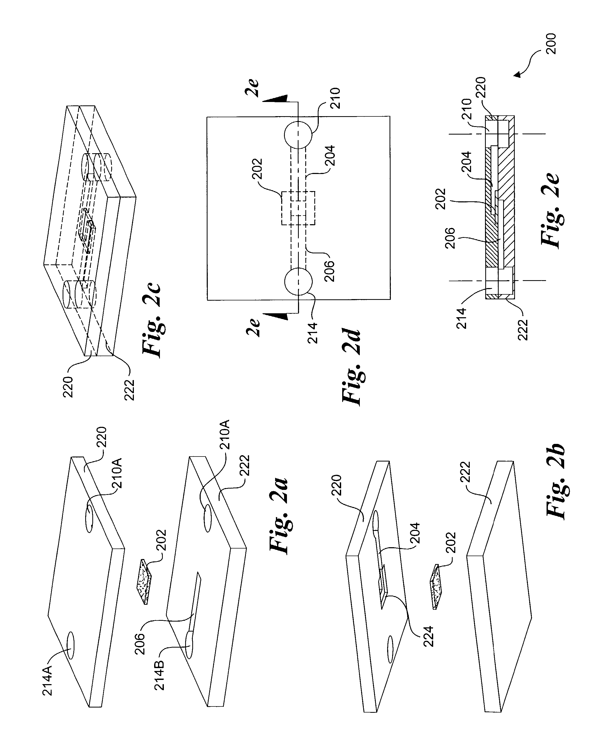
[0014]Embodiments of a microfluidic device with an integrated porous-silicon membrane for molecular sieving, metering, and separations, and methods for fabricating and using the same are described in detail herein. In the following description, numerous specific details are provided, such as the identification of various system components, to provide a thorough understanding of embodiments of the invention. One skilled in the art will recognize, however, that embodiments of the invention can be practiced without one or more of the specific details, or with other methods, components, materials, etc. In still other instances, well-known structures, materials, or operations are not shown or described in detail to avoid obscuring aspects of various embodiments of the invention.

[0015]Reference throughout this specification to “one embodiment” or “an embodiment” means that a particular feature, structure, or characteristic described in connection with the embodiment is included in at leas...


PUM

PropertyMeasurementUnit
pore sizesaaaaaaaaaa
thicknessaaaaaaaaaa
semi-permeableaaaaaaaaaa

Abstract

Microfluidic devices with porous membranes for molecular sieving, metering, and separation of analyte fluids. In one aspect, a microfluidic device includes a substrate having input and output microfluidic channel sections separated by a porous membrane formed integral to the substrate. In another aspect, the porous membrane may comprise a thin membrane that is sandwiched between upper and lower substrate members. The microfluidic device may include one or a plurality of porous membranes. In one embodiment, a plurality of porous membranes having increasingly smaller pores are disposed along portions of a microfluidic channel. In another embodiment, a cascading series of upper and lower channels are employed, wherein each upper/lower channel interface is separated by a respective porous membrane. In another aspect, a porous membrane is rotatably coupled to a substrate within a microfluidic channel via a MEMS actuator to enable the porous membrane to be positioned in filtering and pass-through positions.

Description

TECHNICAL FIELD[0001]This disclosure relates generally to microfluidic devices, and more particularly, but not exclusively, to microfluidic devices having an integrated porous-silicon membrane for filtering molecular components of an influent stream to meter and / or separate chemical and / or biological molecules.BACKGROUND INFORMATION[0002]As the breadth of microchip fabrication technology has continued to expand, an emerging technology associated with miniscule gadgets known as microfluidic devices has taken shape. Microfluidic devices, often comprising miniaturized versions of reservoirs, pumps, valves, filters, mixers, reaction chambers, and a network of capillaries interconnecting the microscale components, are being developed to serve in a variety of deployment scenarios. For example, microfluidic devices may be designed to perform multiple reaction and analysis techniques in one micro-instrument by providing a capability to perform hundreds of operations (e.g. mixing, heating, s...

Claims


Application Information

Patent Timeline
Patent Type & Authority Patents(United States)
IPC IPC(8): B01L3/02B31D3/00B01D61/02G01N37/00B01D61/14B01D61/18B01D61/20B01D69/02B01D71/02B01J19/00B01L3/00B81B1/00
CPCB01D61/022B01D61/18B01D61/20B01D69/02B01D71/02B01L3/502753B01D61/142Y10T436/2575B01D2325/02B01D2325/04B01L2200/12B01L2300/0681B01L2300/087B01L2300/0874B01L2300/0887Y10T436/255Y10T436/25375B01D61/146B01D61/026
Inventor CHAN, SELENASUNDARARAJAN, NARAYANBERLIN, ANDREW A.YAMAKAWA, MINEO
Owner INTEL CORP
Why Eureka
Try Eureka