Flash memory device and manufacturing method thereof

a flash memory device and manufacturing method technology, applied in the direction of semiconductor devices, basic electric elements, electrical appliances, etc., can solve the problems of increasing the complexity of manufacturing memory devices, limiting the ultimate level of integration of devices, and significant drop in the coupling ratio between the control gate and the floating gate of flash memory devices. achieve the effect of simplifying the fabrication process

Inactive Publication Date: 2007-10-09
MACRONIX INT CO LTD
View PDF10 Cites 2 Cited by
  • Summary
  • Abstract
  • Description
  • Claims
  • Application Information

AI Technical Summary

Benefits of technology

[0009]Accordingly, at least one objective of the present invention is to provide a method of manufacturing a flash memory device that utilizes a self-aligned process to save one critical photolithographic step, thereby simplifying the fabrication process.
[0010]At least a second objective of the present invention is to provide a flash memory device having a top-narrow / bottom-wide floating gate so that the gate-coupling ratio can be increased and the device can be miniaturized.
[0014]In the present invention, a self-aligned process is deployed to define the floating gate so that one critical photolithographic processing step is saved. Furthermore, the floating gate structure has a top-narrow / bottom-wide configuration. Hence, the overlapping area between the floating gate and a subsequently formed control gate is increased. Aside from simplifying the fabrication process and increasing the gate-coupling ratio of the stack gate, the flash memory device is further miniaturized.

Problems solved by technology

As a result, there is a significant drop in the coupling ratio between the control gate and the floating gate of the flash memory device.
Although the aforementioned technique of increasing the area of the floating gate can improve the coupling ratio between the floating gate and the control gate, the larger area occupied by the second conductive pattern set a limit on the ultimate level of integration for the devices.
Moreover, the step of forming the second conductive pattern over the first conductive pattern increases the complexity of manufacturing the memory device.
In other words, the process goes against our goal of miniaturizing devices and minimizing the number of fabrication steps.

Method used


Image

  • Flash memory device and manufacturing method thereof
  • Flash memory device and manufacturing method thereof
  • Flash memory device and manufacturing method thereof

Examples


Embodiment Construction

[0021]Reference will now be made in detail to the present preferred embodiments of the invention, examples of which are illustrated in the accompanying drawings. Wherever possible, the same reference numbers are used in the drawings and the description to refer to the same or like parts.

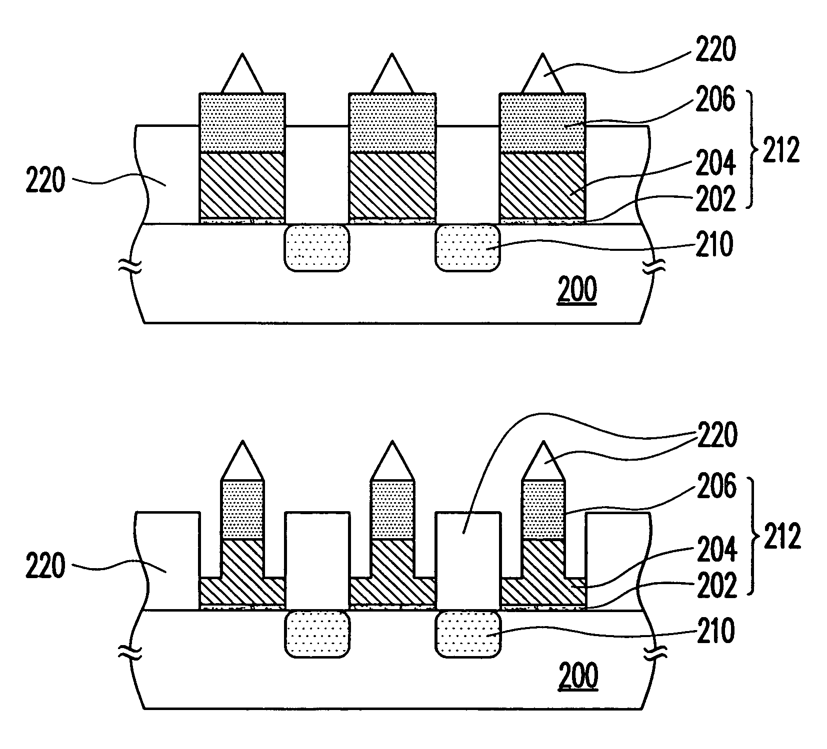
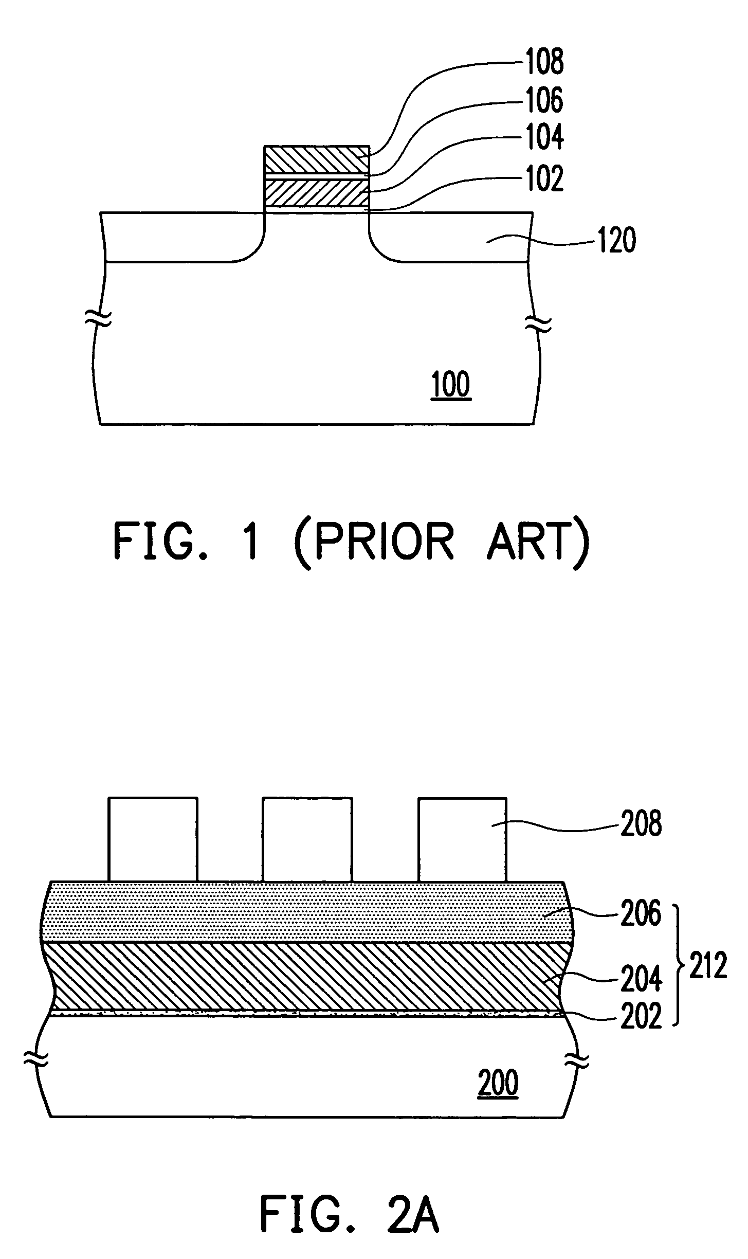
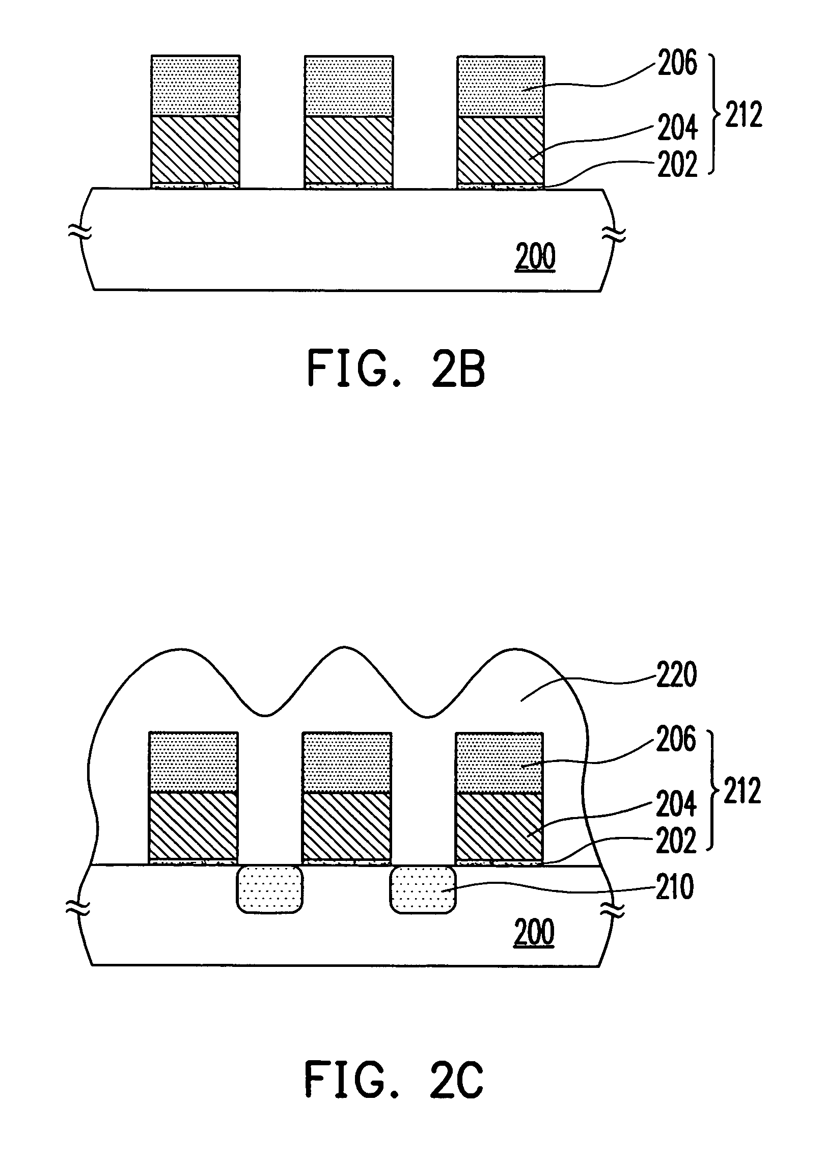
[0022]FIGS. 2A through 2H are schematic cross-sectional views showing the progression of steps for forming a flash memory device according to a first preferred embodiment of the present invention. As shown in FIGS. 2A and 2B, multiple stack structures 212 are first formed over a substrate 200. The steps of forming the stack structures 212, for example, include forming a tunneling oxide layer 202 over a substrate 200 first and forming a first conductive layer 204 over the tunneling oxide layer 202. The first conductive layer 204 is a doped polysilicon layer, for example. A material layer 206 is optionally formed over the first conductive layer 204, and the etching selectivity ratio of the material lay...


PUM


Abstract

A method of manufacturing a flash memory device is provided. Multiple stack structures each comprising a tunneling oxide layer and a first conductive layer are formed over a substrate. Thereafter, multiple embedded doping regions is formed in the substrate between the stack structures. A dielectric layer is formed over the substrate to cover the stack structures and then the dielectric layer is etched back and a portion of dielectric layer is remained on the stack structures. Using a portion of the remaining dielectric layer as a mask, a portion of the first conductive layer is removed. An inter-layer dielectric layer and a second conductive layer are sequentially formed over the first conductive layer. Because a self-aligned process is used to define the floating gate and the floating gate has a narrow-top / wide-bottom configuration, the fabrication process is simplified and the coupling ratio of the stack gate is increased.

Description

BACKGROUND OF THE INVENTION[0001]1. Field of the Invention[0002]The present invention relates to a method of manufacturing memory. More particularly, the present invention relates to a flash memory device and manufacturing method thereof.[0003]2. Description of the Related Art[0004]Flash memory is a type of non-volatile memory that permits multiple data writing, reading and erasing operations. The stored data will be retained even power off. With all these advantages, flash memory has become one of the most widely adopted non-volatile memories for personal computer and electronic equipment.[0005]FIG. 1 is a schematic cross-sectional view of a conventional flash memory device. As shown in FIG. 1, the flash memory mainly comprises a substrate 100, a tunneling oxide layer 102, a floating gate 104, an inter-polysilicon dielectric layer 106, a control gate 108 and a pair of source / drain regions 120. The floating gate 104 is disposed on the substrate 100. The floating gate 104 consists of...

Claims


Application Information

Patent Timeline
Patent Type & Authority Patents(United States)
IPC IPC(8): H01L21/336
CPCH01L21/28114H01L29/42376H01L27/11521H01L27/115H10B69/00H10B41/30
Inventor LAI, ERH-KUNLUE, HANG-TINGSHIH, YEN-HAOHO, CHIA-HUA
Owner MACRONIX INT CO LTD
Why Eureka
Try Eureka