Piezoelectric resonator element, piezoelectric device, method of manufacturing the same, cellular phone device utilizing piezoelectric device, and electronic equipment utilizing piezoelectric device

a piezoelectric device and resonator element technology, applied in the field of piezoelectric resonator elements, piezoelectric devices, methods of manufacturing them, cellular phones, etc., can solve the problems of difficult to form the sharp pattern of the lower layer when etching, the frequency tolerance of temperature changes is large, and the temperature characteristic is improved. , the effect of reducing the coefficient of temperature characteristic curv

Inactive Publication Date: 2007-10-09
SEIKO EPSON CORP
View PDF17 Cites 63 Cited by
  • Summary
  • Abstract
  • Description
  • Claims
  • Application Information

AI Technical Summary

Benefits of technology

[0014]Thus, since the thickness t of the lower layer is in the above range, the second order coefficient of the temperature characteristic curve is decreased considerably so that a flat part in the temperature characteristic is obtained. Therefore, the changes of frequency tolerance due to temperature changes can be reduced. Because the thickness t of the lower layer is large as described above, by forming electrodes for driving, stress is caused in the forming portion so as to affect the oscillation characteristic, and thus the temperature characteristic is improved.
[0048]Thus, since the thickness t of the lower layer is in the above range, the second order coefficient of the temperature characteristic curve is decreased considerably so that a flat part in the temperature characteristic is obtained. Therefore, the changes of frequency tolerance due to temperature changes can be reduced. Because the thickness t of the lower layer is large as described above, by forming electrodes for driving, stress is caused in the forming portion so as to affect the oscillation characteristic, and thus the temperature characteristic is improved.

Problems solved by technology

Therefore, there is a problem that the changes of frequency tolerance due to temperature changes become large.
Moreover, if the thickness t of the lower layer is 0.3 micrometers or more, side etching by an etchant for the lower layer is intensely caused when forming an electrode pattern by etching, so that the patterning of electrodes with high accuracy becomes impossible.
Furthermore, if the thickness t of the lower layer is 0.11 micrometers or more, side etching against the lower layer is easily caused when forming an electrode pattern by etching, and thus it may become hard to form the sharp pattern of the lower layer when etching.
Moreover, if the thickness t of the lower layer is 0.3 micrometers or more, side etching by an etchant for the lower layer is intensely caused when forming an electrode pattern by etching, so that the patterning of electrodes with high accuracy becomes impossible.

Method used


Image

  • Piezoelectric resonator element, piezoelectric device, method of manufacturing the same, cellular phone device utilizing piezoelectric device, and electronic equipment utilizing piezoelectric device
  • Piezoelectric resonator element, piezoelectric device, method of manufacturing the same, cellular phone device utilizing piezoelectric device, and electronic equipment utilizing piezoelectric device
  • Piezoelectric resonator element, piezoelectric device, method of manufacturing the same, cellular phone device utilizing piezoelectric device, and electronic equipment utilizing piezoelectric device

Examples


Embodiment Construction

[0062]Preferred embodiments of the present invention will be described below with reference to the drawings.

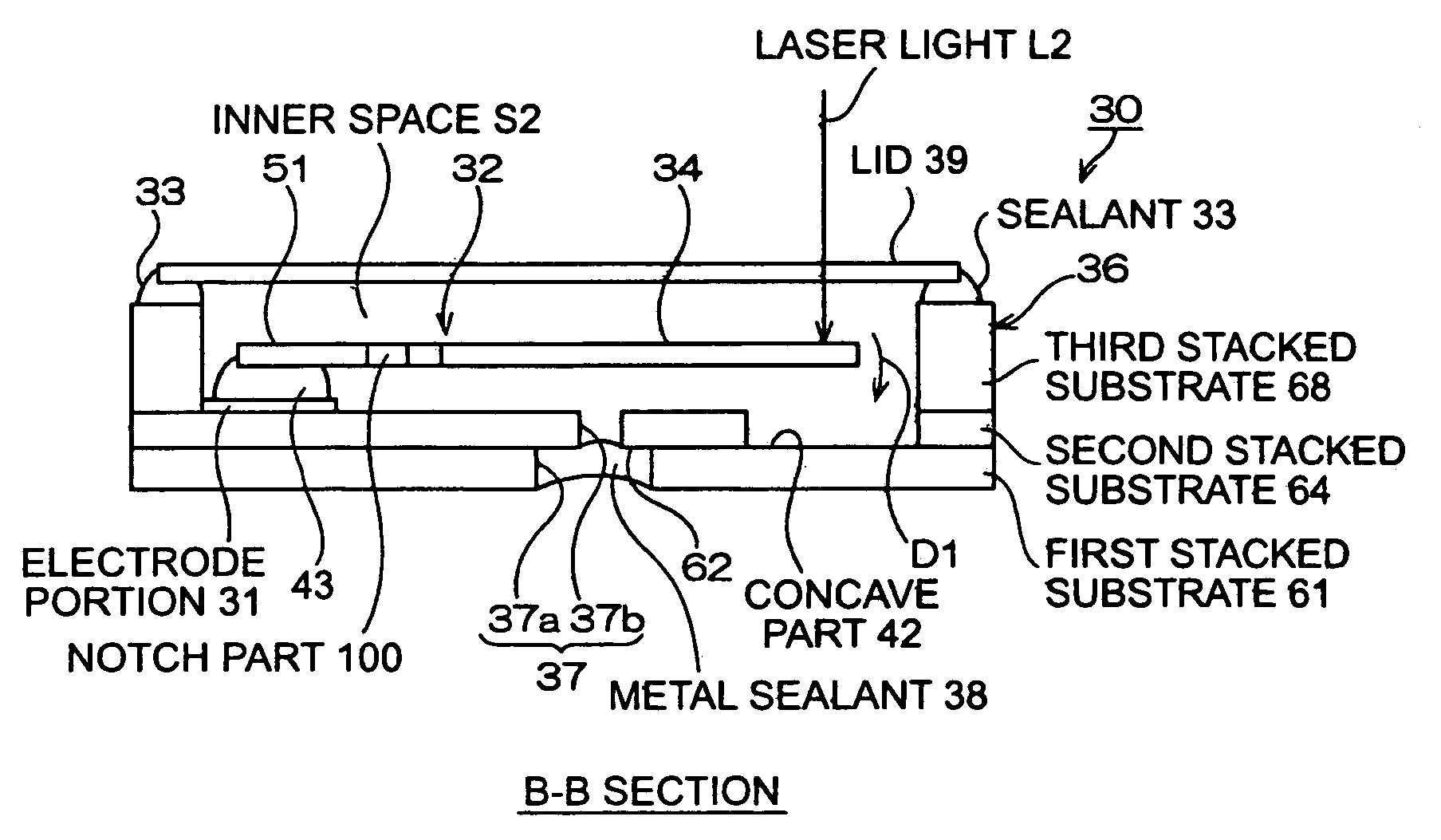
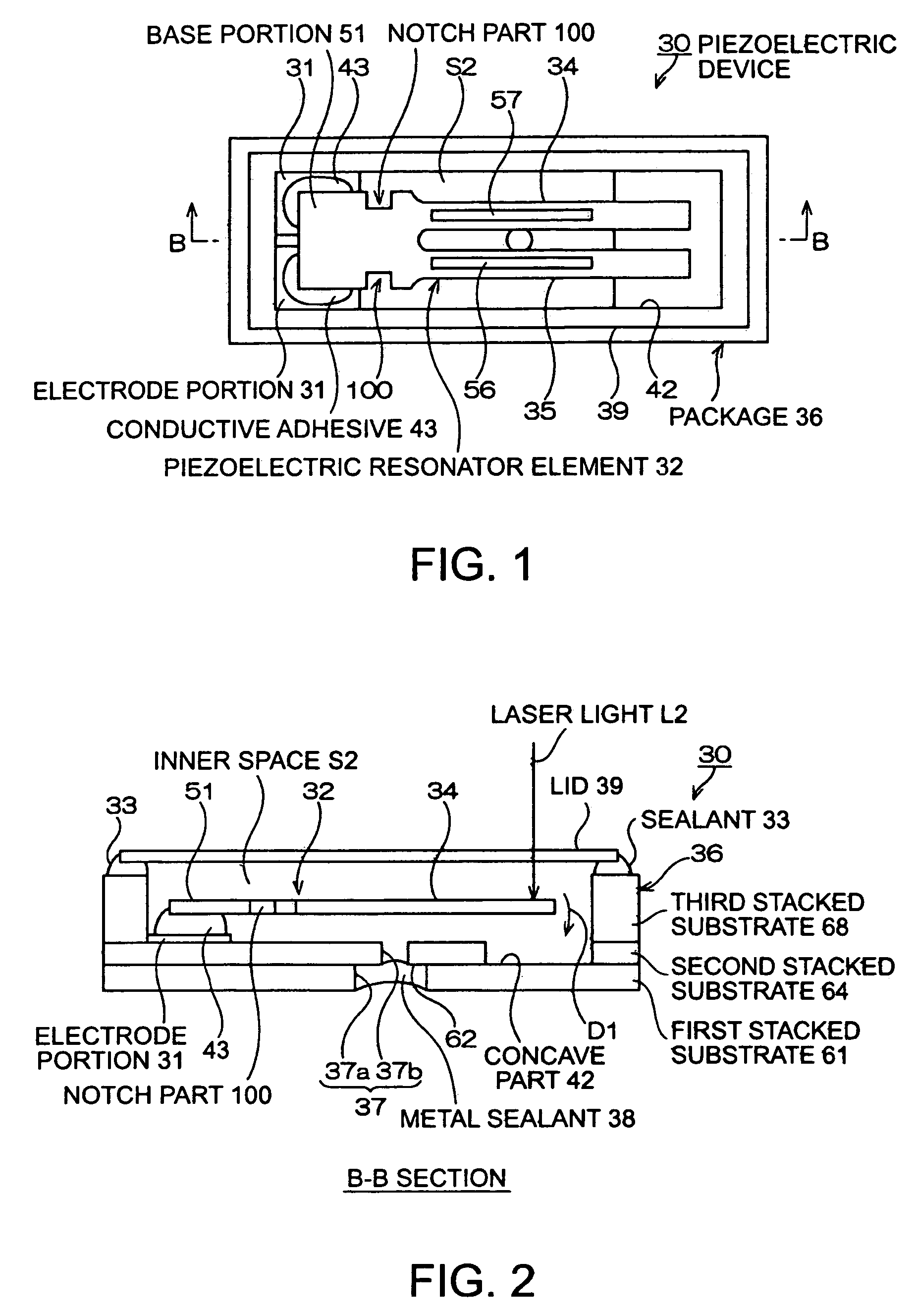
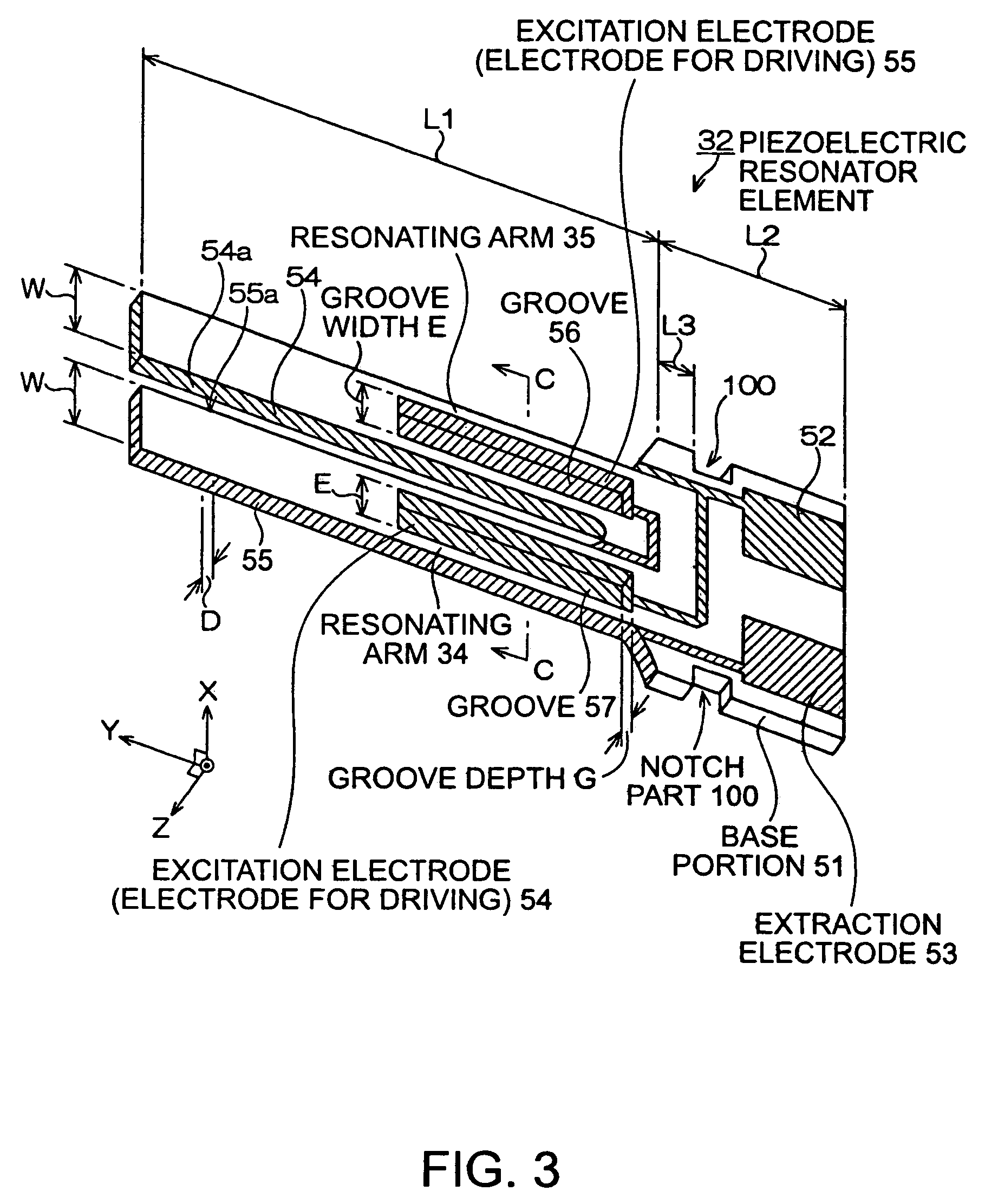
[0063]FIGS. 1 and 2 show an embodiment of a piezoelectric device of the present invention. FIG. 1 is a schematic plain view thereof, and FIG. 2 is a schematic sectional view along B-B line of FIG. 1.

[0064]Referring to FIGS. 1 and 2, in a piezoelectric device 30, an example in which a crystal resonator is constituted is shown. The piezoelectric device 30 contains a piezoelectric resonator element 32 in a package 36. The package 36 is formed by stacking a plurality of substrates formed by shaping ceramic green sheets composed of aluminum oxide as an insulating material, and then sintering it, for example. A given hole is formed inside each of the plurality of substrates in order to form a given inner space S2 inside when stacked.

[0065]This inner space S2 is a housing space to house the piezoelectric resonator element.

[0066]Namely, as shown in FIG. 2, in this embodiment, the pack...


PUM


Abstract

A piezoelectric resonator element is provided including a base portion and a plurality of resonating arms extending from the base portion. A notch part is formed in the base portion. Grooves are formed in the front and back surfaces of the resonating arms. A driving electrode is provided at least in the grooves of the resonating arms. The driving electrode has a lower layer and an electrode layer formed on the lower layer. The thickness t of the lower layer is in the range 0.07<t<0.3 micrometers.

Description

RELATED APPLICATIONS[0001]This application claims priority to Japanese Patent Application No. 2003-367743 filed Oct. 28, 2003 which is hereby expressly incorporated by reference herein in its entirety.BACKGROUND[0002]1. Field of the Invention[0003]The present invention relates to a piezoelectric resonator element, a piezoelectric device, a method of manufacturing them, a cellular phone, and electronic equipment that utilize a piezoelectric device.[0004]2. Related Art[0005]In small information equipment such as a hard disc drive (HDD), a mobile computer, or an integrated circuit (IC) card, and mobile communication equipment such as a cellular phone, a car-phone, or a paging system, a piezoelectric device such as a crystal resonator and a crystal oscillator that contains a piezoelectric resonator element in a package has been widely used.[0006]A piezoelectric resonator element contained in a conventional piezoelectric device has a structure including a base portion and a pair of reson...

Claims


Application Information

Patent Timeline
Patent Type & Authority Patents(United States)
IPC IPC(8): H01L41/08H01L41/09H01L41/18H01L41/22H01L41/23H01L41/29H01L41/332H03B5/32H03H3/02H03H9/19H03H9/21H03H9/215
CPCH03H9/21H03H9/19H03B5/32
Inventor TANAYA, HIDEOJOKURA, TOSHINARIOSHIRO, ATSUSHI
Owner SEIKO EPSON CORP
Why Eureka
Try Eureka