Semiconductor light emitting device

a technology of light-emitting devices and semiconductors, which is applied in the direction of semiconductor/solid-state device details, point-like light sources, lighting and heating apparatus, etc., can solve the problems of poor light-emitting efficiency to degrade the light-emitting element in the worst case, increase the temperature, and inability to achieve efficient heat-emitting, etc., to achieve reliable heat-emitting and efficient release of hea

Active Publication Date: 2007-10-16
SHARP KK
View PDF12 Cites 58 Cited by
  • Summary
  • Abstract
  • Description
  • Claims
  • Application Information

AI Technical Summary

Benefits of technology

[0012]In view of the foregoing, an object of the present invention is to provide a semiconductor light emitting device that can achieve heat conduction reliably towards a reflector and that can release heat efficiently from the reflector to the air.

Problems solved by technology

However, a large current flow to the semiconductor light emitting device will cause increase of the temperature of the light emitting element per se, leading to poor light emitting efficiency to degrade the light emitting element in the worst case.
Therefore, a dedicated jig to position the reflector at predetermined site was required since heat conduction cannot be achieved efficiently if the position of the reflector is deviated.
Thus, there was the problem that heat cannot be released efficiently to the air from the reflector.

Method used


Image

  • Semiconductor light emitting device
  • Semiconductor light emitting device
  • Semiconductor light emitting device

Examples


first embodiment

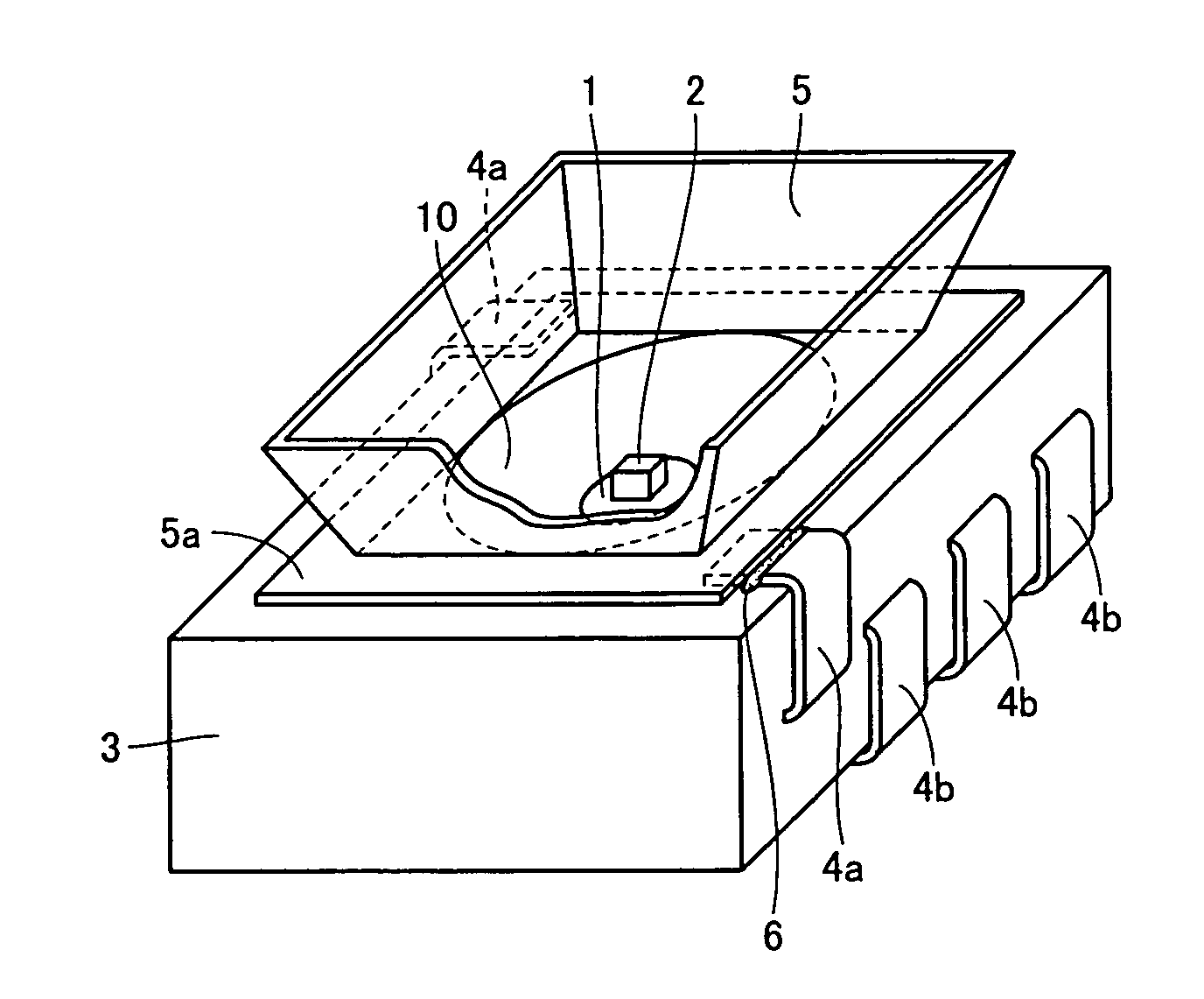
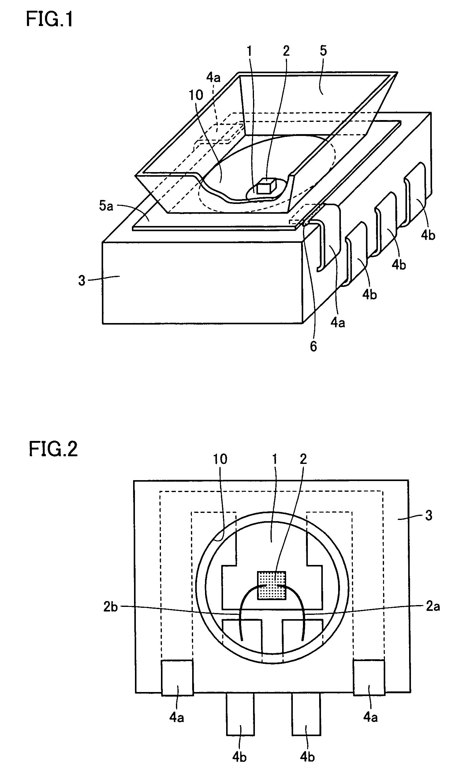
[0042]Referring to FIGS. 1 and 2, a semiconductor light emitting device according to a first embodiment of the present invention has an opening 10 formed at a top face of a resin package 3. A light emitting element 2 is die-bonded to a region of a lead frame 1 exposed at the bottom of opening 10. At a top face of resin package 3, a reflector 5 is attached to direct the light emitted by the light emitting element 2 towards a predetermined direction. Reflector 5 is attached such that its entirety is exposed to the air.

[0043]Respective lead terminals 4a and 4b of lead frame 1 are disposed so as to project from each of the two opposite side regions of resin package 3. Among the plurality of lead terminals 4a and 4b, a predetermined lead terminal 4a connected to the region where light emitting element 2 is die-bonded is bent upward. The leading end of the bent lead terminal 4a is soldered by, for example, solder paste 6 to a fringe portion identified as an attach region 5a of reflector 5...

second embodiment

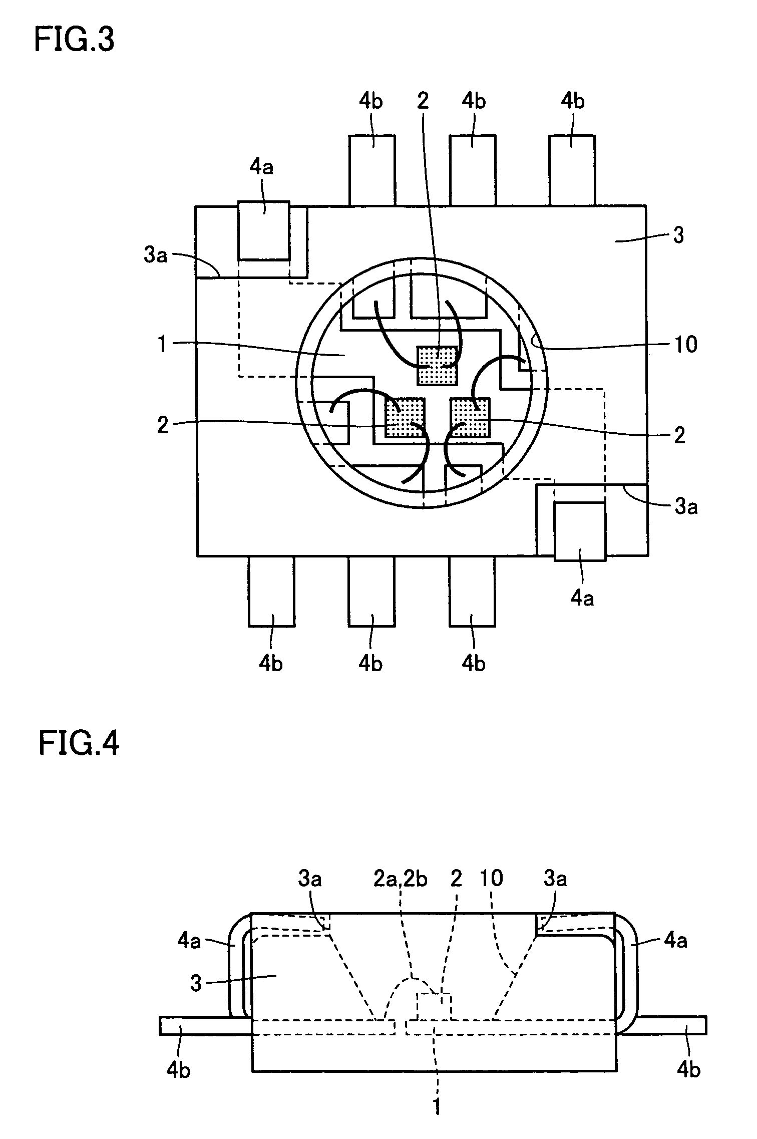
[0052]A semiconductor light emitting device according to a second embodiment of the present invention is directed to fixing the reflector more stably to the resin package.

[0053]Referring to FIGS. 3 and 4, a groove 3a is formed in advance at the top face of resin package 3 such that the top plane of lead terminal 4a is substantially flush with the top face of resin package 3 with lead terminal 4a connected to reflector 5 (refer to FIG. 1) in a bending status. The remaining configuration of the semiconductor light emitting device of the second embodiment is similar to the semiconductor light emitting device shown in FIG. 1. Therefore, the same elements have the same reference characters allotted, and description thereof will not be repeated.

[0054]In the semiconductor light emitting device of the second embodiment, lead terminal 4a connected to reflector 5 is received in groove 3a provided at the top face of resin package 3 by being bent towards the top face of resin package 3. Accordi...

third embodiment

[0056]A semiconductor light emitting device according to a third embodiment of the present invention has a reflector formed integrally with the lead frame. Referring to FIG. 5, a portion to become reflector 5 is formed integrally with the leading end of lead terminal 4a. This portion to become the reflector is formed in a state (shape) in which the reflector is spread out in an unfolded manner corresponding to an expansion plan, including four reflector bodies 55 in the present embodiment.

[0057]A projection 55a is provided at one of adjacent reflector bodies 55. A notch 55b to be engaged with projection 55a is provided at the other of the adjacent reflector bodies 55.

[0058]By bending each reflector body 55 and holding projection 55a of reflector body 55 under engagement with notch 55b of an adjacent reflector body 55, reflector 5 is assembled. A semiconductor light emitting device having reflector 5 at the top face of resin package 3 is obtained, as shown in FIG. 6. The remaining el...


PUM


Abstract

A light emitting element is die-bonded to a portion of a lead frame exposed at the bottom of an opening formed at a top face of a resin package. A reflector to direct light emitted from the light emitting element towards a predetermined direction is attached to the top face of the resin package. Lead terminals are arranged so as to protrude from two opposite side regions of the resin package. A predetermined lead terminal among the plurality of lead terminals, connected to a portion where the light emitting element is die-bonded, is bent upwards, and soldered to the reflector by solder paste.

Description

[0001]This nonprovisional application is based on Japanese Patent Application No. 2003-419585 filed with the Japan Patent Office on Dec. 17, 2003, the entire contents of which are hereby incorporated by reference.BACKGROUND OF THE INVENTION[0002]1. Field of the Invention[0003]The present invention relates to semiconductor light emitting devices, and more particularly, to a semiconductor light emitting device including a light emitting element.[0004]2. Description of the Background Art[0005]In general semiconductor light emitting devices employed as the illumination device of a camera, the backlight of a liquid crystal display device, and the like, much current is conducted to achieve higher luminosity. However, a large current flow to the semiconductor light emitting device will cause increase of the temperature of the light emitting element per se, leading to poor light emitting efficiency to degrade the light emitting element in the worst case.[0006]Therefore, measures to release ...

Claims


Application Information

Patent Timeline
Patent Type & Authority Patents(United States)
IPC IPC(8): H01L27/15F21V29/00F21V1/00F21Y101/02H01L33/60H01L33/62H01L33/64
CPCH01L33/60H01L33/486H01L2224/48091H01L2224/48247H01L2924/00014
Inventor CHIKUGAWA, HIROSHIYAMAMOTO, YOSHIHIKOKAMETANI, EIJI
Owner SHARP KK
Why Eureka
Try Eureka