Thermal conductive substrate and semiconductor module using the same

a technology of thermal radiation substrate and semiconductor module, which is applied in the direction of semiconductor devices, solid-state devices, basic electric elements, etc., can solve the problems of module rise, insufficient resistance to voltage, and inability to resist voltage, so as to improve thermal radiation properties, reduce cracks or peeling, and achieve high-reliability substrates. the effect of high efficiency

Inactive Publication Date: 2005-10-25
PANASONIC CORP
View PDF27 Cites 46 Cited by
  • Summary
  • Abstract
  • Description
  • Claims
  • Application Information

AI Technical Summary

Benefits of technology

[0014]A thermal conductive substrate obtained according to the present invention is a circuit substrate comprising at least a wiring pattern, an electrical insulating layer and a thermal radiation layer, in which the substrate warps to protrude toward the thermal radiation board as the temperature rises. Accordingly, thermal radiation from a semiconductor module comprising the thermal conductive substrate to the external thermal radiation member is not hindered even if the temperature rises at a time of operation of the module, and thus, a thermal conductive substrate having improved thermal radiation property can be provided. Furthermore, the substrate will have less cracks or peeling caused by warping at a high temperature or by stress occurring in the electrical insulating layer, and thus, a highly reliable substrate can be obtained. Use of the thermal conductive substrate according to the present invention will provide a highly reliable semiconductor module with a good thermal radiation property.

Problems solved by technology

Therefore, the spacing between the circuit pattern and the metal plate is susceptible to noise, and the withstand voltage is insufficient.
As a result, the thermal resistance is raised and the temperature of the module rises so much that abnormal operation and failure of the components result.
However, stress will occur at a time of fixing, which causes fractures and cracks of the insulating layer.
Otherwise, peeling occurs between either the wiring pattern or the thermal radiation board and the insulating layer.
However, since the circuit substrate is constructed by laminating layers of various materials, a warping degree of the board varies depending on the temperature.
Therefore, even if the circuit substrate is contacted sufficiently with the external thermal radiation member at the time of fixing, the circuit substrate warps due to the temperature rise during the operation of the semiconductor module so that the contact area is reduced to cause thermal runaway of the semiconductor module.
As a result, fractures or cracks occur in the board, which results in insulation failure or degradation in the reliability.

Method used


Image

  • Thermal conductive substrate and semiconductor module using the same
  • Thermal conductive substrate and semiconductor module using the same
  • Thermal conductive substrate and semiconductor module using the same

Examples


first embodiment

(First Embodiment)

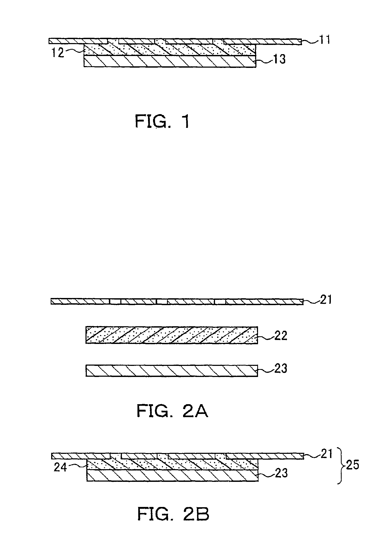
[0036]FIG. 1 is a cross-sectional view showing a structure of a thermal conductive substrate in one embodiment of the present invention. This substrate is composed of a lead frame 11 as a wiring pattern, an electrical insulating layer 12 and a thermal radiation board 13. The electrical insulating layer 12 is composed of a thermal conductive mixture containing an inorganic filler and a thermosetting resin. The content of the inorganic filler is preferred to be in a range from 70 wt % to 95 wt %, and especially, in a range from 85 wt % to 95 wt %. When the content of the blended inorganic filler is less than the above-identified range, a thermal radiation property of the substrate deteriorates. The thermal expansion coefficient of the electrical insulating layer 12 is increased when the inorganic filler content is reduced, and this hinders the tendency of the substrate to warp and protrude toward the thermal radiation board with the rise of temperature. When the cont...

second embodiment

(Second Embodiment)

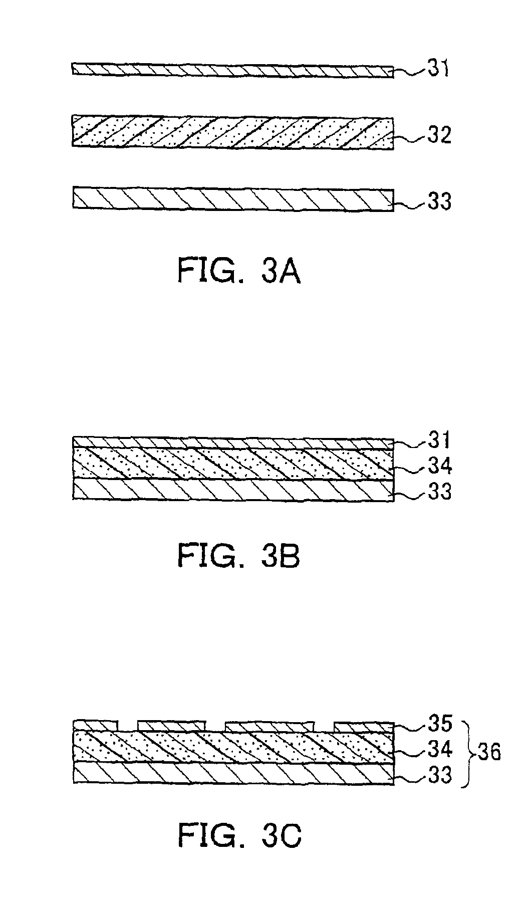
[0047]FIG. 3A-3C are cross-sectional views of respective steps to show a method of manufacturing a thermal conductive substrate in another embodiment of the present invention. In FIG. 3A, 31 denotes a metal foil, 32 denotes a thermal conductive mixture as described in the first embodiment, and 33 denotes a thermal radiation board as described in the first embodiment. These components are laminated and subjected to heat and pressure as shown in FIG. 3A. The thermosetting resin in the thermal conductive mixture 32 is cured to be an electrical insulating layer 34, and the electrical insulating layer 34 is integrated with the metal foil 31 and the thermal radiation board 33 by adhesion as shown in FIG. 3B. Subsequently, the metal foil 31 is patterned to provide a wiring pattern 35, so that a completed thermal conductive substrate 36 is provided as shown in FIG. 3C. If required, this process can be followed by, for example, a solder-resist printing, soldering of an ext...

third embodiment

(Third Embodiment)

[0049]FIGS. 4A-4E are cross-sectional views of respective steps to show a method of manufacturing a thermal conductive substrate in still another embodiment of the present invention. In FIG. 4A, a metal foil 41 is adhered onto a releasing film 43 via an adhesive layer 42. This metal foil 41 is patterned to provide a wiring pattern 44 as shown in FIG. 4B. The wiring pattern 44 is reversed to be laminated on a thermal conductive mixture 45 and a thermal radiation board 46 as described in the first embodiment in this order, so that the wiring pattern 44 is contacted with the thermal conductive mixture 45 as shown in FIG. 4C. The laminate is subjected to heat and pressure so that the thermosetting resin in the thermal conductive mixture 45 is cured to become an electrical insulating layer 47, and simultaneously, the wiring pattern 44 is integrated with the thermal radiation board 46 by adhesion as shown in FIG. 4D. Later, the releasing film 43 and the adhesive layer 42...


PUM

PropertyMeasurementUnit
elastic modulusaaaaaaaaaa
thicknessaaaaaaaaaa
temperatureaaaaaaaaaa

Abstract

A semiconductor module includes a circuit substrate composed of a wiring pattern, an electrical insulating layer and a thermal radiation board, and in use is fixed to an external thermal radiation member, in which the electrical insulating layer is composed of a thermal conductive mixture containing 70-95 wt % of an inorganic filler and 5-30 wt % of a thermosetting resin. A warping degree of the circuit substrate with respect to the external thermal radiation member is at most 1/500 of a length of the substrate, and the circuit substrate warps to protrude toward the thermal radiation board as the temperature rises. Accordingly, the thermal radiation property does not deteriorate even when the temperature rises in use. At a time of fixing the circuit substrate to the external thermal radiation member, the thermal resistance is kept to be a sufficiently low level. The thermal resistance is kept in a low level without sacrificing the contact between a module and the external thermal radiation member even at a high temperature during an operation of the device or the like, and the thermal conductive substrate is resistant to fractures or cracks and thus is highly reliable.

Description

BACKGROUND OF THE INVENTION[0001]1. Field of the Invention[0002]The present invention relates to circuit substrates used for various electric and electronic apparatuses and also semiconductor modules using the same. Particularly, the present invention relates to thermal conductive substrates suitable for apparatuses that are used in a field of power electronics or the like and require improved thermal radiation property.[0003]2. Description of Related Art[0004]Recently, as high performance and miniaturization of electronic apparatuses have been required, high density and high performance semiconductors have been sought. Consequently, circuit substrates for mounting thereof also have been required to be small and of high density. As a result, it is important to design circuit substrates taking the thermal radiation property into consideration. While many conventional printed circuit boards are made of a glass-epoxy resin, a well known technique for improving the thermal radiation pro...

Claims


Application Information

Patent Timeline
Patent Type & Authority Patents(United States)
IPC IPC(8): H01L23/34H01L23/373H05K1/05H01L23/14
CPCH01L23/3737H05K1/056H01L2924/09701H01L2224/16225H01L2924/19105H01L2924/00014H01L23/3735H01L2224/0401H01L23/14
Inventor HIRANO, KOICHIYAMASHITA, YOSHIHISANAKATANI, SEIICHI
Owner PANASONIC CORP
Why Eureka
Try Eureka