Microstructure for use in Raman spectrometry and production process for the microstructure

a microstructure and raman spectrometry technology, applied in the field of microstructures, can solve the problems of difficult detection of raman scattered light, low light intensity, and inability to make the head portions of minute metal particles protrude sufficiently high, and achieve high quality, easy manufacturing, and high performance.

Inactive Publication Date: 2007-10-30
FUJIFILM HLDG CORP +1
View PDF3 Cites 39 Cited by
  • Summary
  • Abstract
  • Description
  • Claims
  • Application Information

AI Technical Summary

Benefits of technology

[0007]An object of the present invention is to provide a microstructure having a function of increasing the intensity of Raman scattered light, exhibiting high performance, having high quality, being easy to manufacture, and enabling stable supply.
[0008]Another object of the present invention is to provide a process for producing a microstructure having a function of increasing the intensity of Raman scattered light, exhibiting high performance, having high quality, being easy to manufacture, and enabling stable supply.
[0009]Still another object of the present invention is to provide a process for performing Raman spectrometry by using a microstructure which has a function of increasing the intensity of Raman scattered light, exhibits high performance, has high quality, is easy to manufacture, and enables stable supply.

Problems solved by technology

The Raman scattered light has a very low intensity, and therefore detection of the Raman scattered light is generally not easy.
Therefore, it is not easy to make the head portions of the minute metal particles protrude sufficiently high.

Method used


Image

  • Microstructure for use in Raman spectrometry and production process for the microstructure
  • Microstructure for use in Raman spectrometry and production process for the microstructure
  • Microstructure for use in Raman spectrometry and production process for the microstructure

Examples


Embodiment Construction

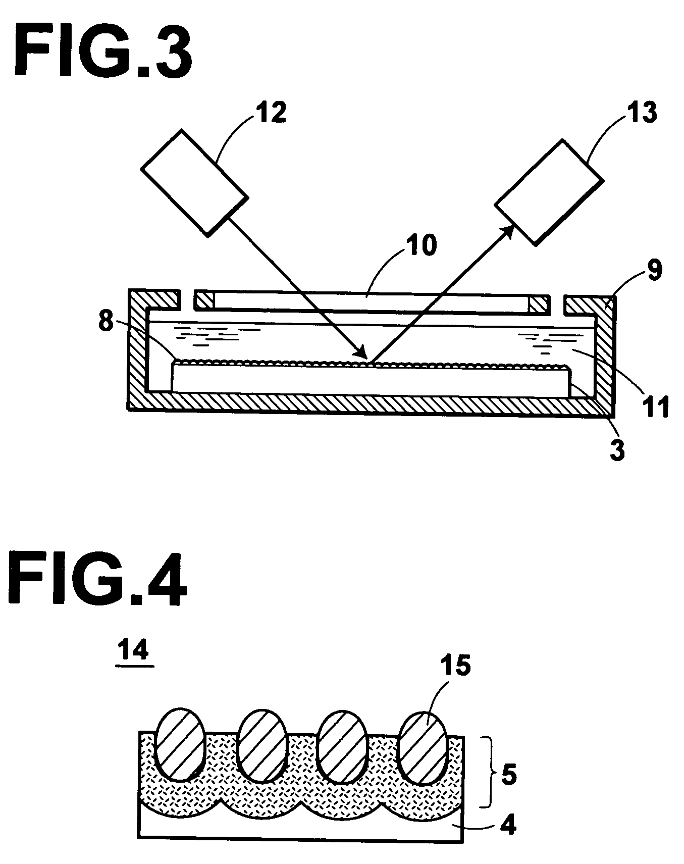
[0042]An embodiment of the present invention is explained in detail below with reference to the drawings.

Microstructure

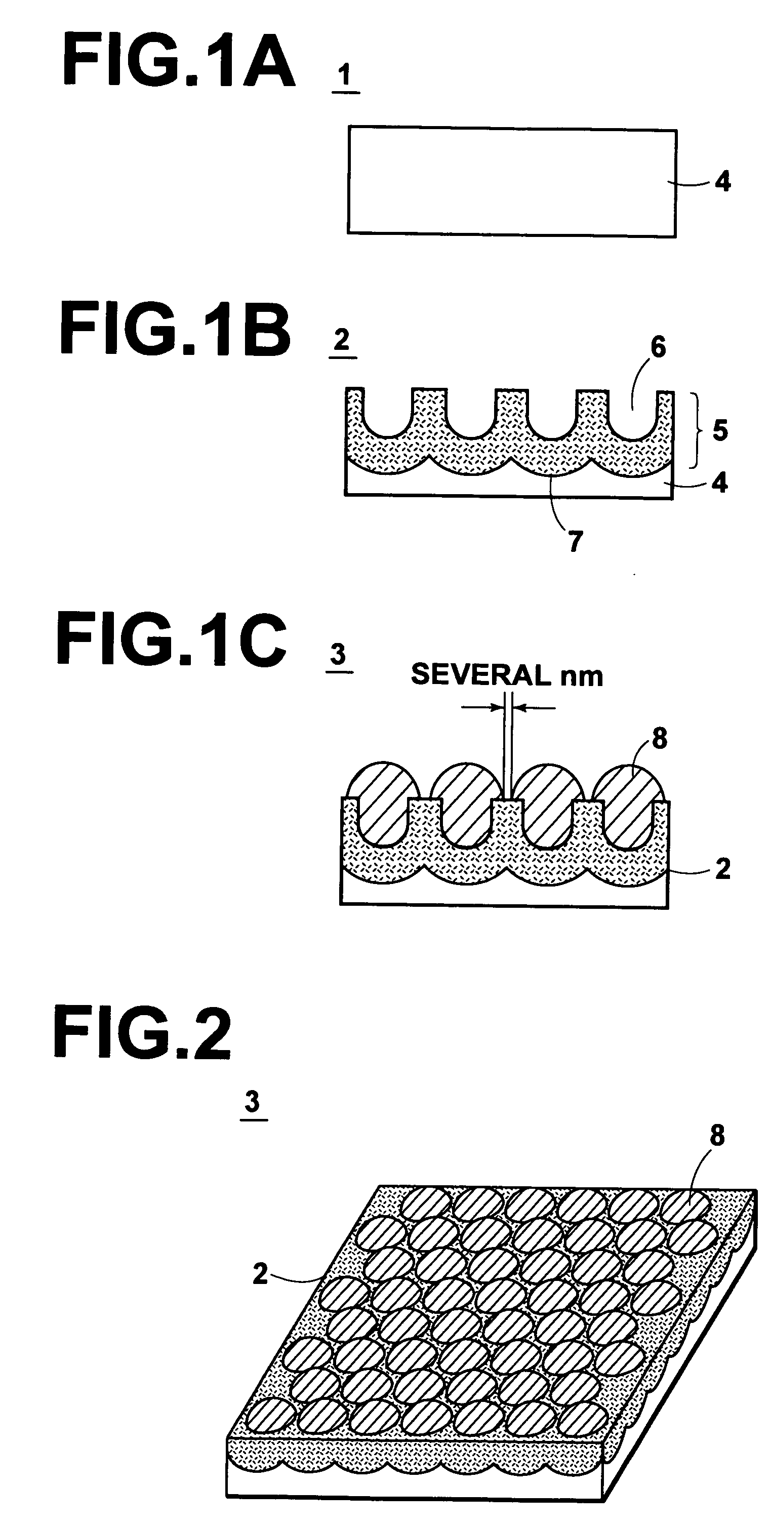
[0043]First, a process for producing a microstructure according to the present embodiment is explained with reference to FIGS. 1A to 1C, which are schematic cross-sectional views of structures in representative stages of a process for producing a microstructure according to the embodiment of the present invention. Although the microstructure according to the present invention can be formed by using various processes, a process using an aluminum substrate is explained below.

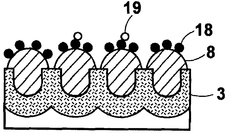
[0044]FIG. 1A is a schematic cross-sectional view of a substrate 1 before the process for producing the microstructure is started. In this example, the substrate 1 is made of only an aluminum layer 4. Alternatively, the substrate 1 may be constituted by a support made of a material other than aluminum and a layer of aluminum or an aluminum alloy formed on the support. That is, only the surface lay...


PUM

PropertyMeasurementUnit
diametersaaaaaaaaaa
diametersaaaaaaaaaa
diametersaaaaaaaaaa

Abstract

In a microstructure: minute pores are formed at a surface of a substrate in such a manner that the minute pores are dispersedly distributed over the surface, and the gaps between the minute pores are 1 micrometer or smaller; minute metal particles are arranged at the minute pores and have such sizes that the minute metal particles can cause localized plasmon resonance; the minute metal particles have head portions protruding from the surface; and the diameters of the head portions are greater than the diameters of the minute pores. In Raman spectrometry, a specimen material is absorbed by the surface from which the head portions protrude, light is applied to the surface, and a spectrum of scattered light is obtained.

Description

BACKGROUND OF THE INVENTION[0001]1. Field of the Invention[0002]The present invention relates to a microstructure suitable for use in Raman spectrometry. The present invention also relates to a process for producing a microstructure suitable for use in Raman spectrometry. The present invention further relates to a process for performing Raman spectrometry and a Raman spectrometric system using the above microstructure.[0003]2. Description of the Related Art[0004]In Raman spectrometry, a material is irradiated with monochromatic excitation light, scattered light (called Raman scattered light) having wavelengths different from the wavelength of the excitation light is obtained, and a spectrum of the Raman scattered light (called Raman spectrum) is analyzed. The Raman scattered light has a very low intensity, and therefore detection of the Raman scattered light is generally not easy. However, it is reported that the intensity of the Raman scattered light is increased by a factor of 104...

Claims


Application Information

Patent Timeline
Patent Type & Authority Patents(United States)
IPC IPC(8): H01L21/76G01J3/44B82B1/00B82B3/00G01N21/65
CPCG01N21/658
Inventor NAYA, MASAYUKI
Owner FUJIFILM HLDG CORP
Why Eureka
Try Eureka