Semiconductor device having through electrode and method of manufacturing the same

a technology of semiconductor devices and electrodes, which is applied in the direction of semiconductor devices, semiconductor/solid-state device details, electrical apparatus, etc., can solve the problems of reducing the yield and reliability of semiconductor devices, difficult processing, and large size of semiconductor devices, and achieves high reliability, easy formation, and reduced size

Active Publication Date: 2007-10-30
RENESAS ELECTRONICS CORP
View PDF1 Cites 17 Cited by
  • Summary
  • Abstract
  • Description
  • Claims
  • Application Information

AI Technical Summary

Benefits of technology

[0012]An object of the present invention is to provide a semiconductor device having a through electrode which enables a size reduction, has high reliability and is easily formed even with a large aspect ratio, and to provide a method of manufacturing the same.
[0015]According to a construction described above, the columnar conductive portion to be a through electrode can be formed with a method of manufacturing a semiconductor device described below. Therefore, a semiconductor device having a through electrode with high reliability can be formed.
[0021]According to the method as described above, reliability of the semiconductor device having a through electrode is increased because a step of depositing a film on an inner wall of the concave portion of the concave substrate is not required, which step is difficult to control. In addition, since an insulation film having a low permittivity and a large thickness can be used, high-speed performance of the semiconductor device is not suppressed by defectiveness of the insulation film. In addition, the temporary substrate having the columnar conductive portion formed therein functions as a support body when the back surface of the semiconductor device is polished. Therefore, as a separate step of attaching the support body is not required according to the method described above, manufacturing steps of a semiconductor device can be decreased.

Problems solved by technology

It is, however, extremely difficult to process as described above.
When the covering property of the insulation film described above is not good, electrical leakage in the semiconductor substrate and a malfunction of a semiconductor circuit will result in reduced yield and reliability of the semiconductor device.
In addition, when the covering property of the seed layer described above is not good, the yield of the semiconductor device will be reduced because, during the electroplating, a void is generated in the metal to be the through electrode.
Therefore, the metal is formed sufficiently in an upper portion of the second hole, in which portion the agent solution flows at a high rate, while the metal is formed insufficiently in a portion near a bottom surface of the second hole, in which portion the agent solution flows at a low rate.
Enlargement of openings of the first and second holes, however, inhibits a size reduction of the semiconductor device.
This leads to decreased rigidity of the semiconductor substrate.
As a result, reliability of the semiconductor device is decreased.
Furthermore, the support board and an adhesive for adhering the support board to the semiconductor device have limitations such that they must have heat and chemical resistances and must allow easy peeling of the support board from the semiconductor device.

Method used


Image

  • Semiconductor device having through electrode and method of manufacturing the same
  • Semiconductor device having through electrode and method of manufacturing the same
  • Semiconductor device having through electrode and method of manufacturing the same

Examples


first embodiment

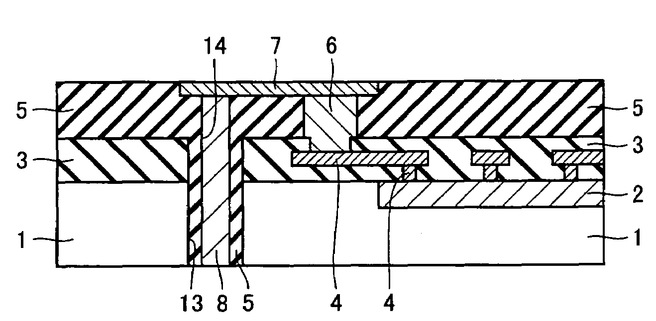
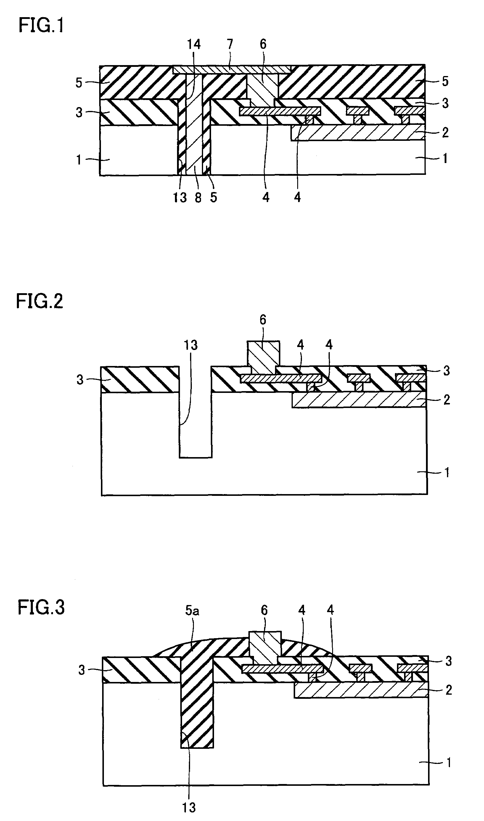
[0070]A structure of a semiconductor device according to a first embodiment is described using FIG. 1.

[0071]As shown in FIG. 1, the semiconductor device of this embodiment includes a semiconductor substrate 1. A semiconductor circuit 2 is formed in semiconductor substrate 1. An insulation film 3 is formed so as to cover a surface of semiconductor substrate 1 including a surface of semiconductor circuit 2. An internal interconnection 4 is formed in insulation film 3. Internal interconnection 4 is connected to semiconductor circuit 2. An insulation film 5 is formed on insulation film 3. In addition, a bump 6 is provided to penetrate through insulation film 5 in a vertical direction. Bump 6 is connected to internal interconnection 4.

[0072]A conductive portion 7 is also formed in insulation film 5. Main surfaces of conductive portion 7 and insulation film 5 are on the same plane. That is, conductive portion 7 is exposed on a surface of insulation film 5. In addition, conductive portion ...

second embodiment

[0088]A structure of a semiconductor device according to a second embodiment will now be described using FIG. 10.

[0089]The semiconductor device according to this embodiment as shown in FIG. 10 has a structure similar to that of the semiconductor device according to the first embodiment shown in FIG. 1. The semiconductor device of this embodiment, however, is different from the semiconductor device of the first embodiment in the following points.

[0090]In the semiconductor device according to this embodiment, an internal interconnection 40 is provided in place of internal interconnection 4. A portion of internal interconnection 40 is defined as a connection portion 41. A conductive portion 70 is connected to an upper surface of connection portion 41. A columnar conductive portion 80 is connected to a lower surface of conductive portion 70. That is, the semiconductor device of this embodiment has a nail-like through electrode 220, as shown in FIG. 10. It is to be noted that, in the sec...

third embodiment

[0102]A structure of a semiconductor device according to a third embodiment will now be described using FIGS. 20-25.

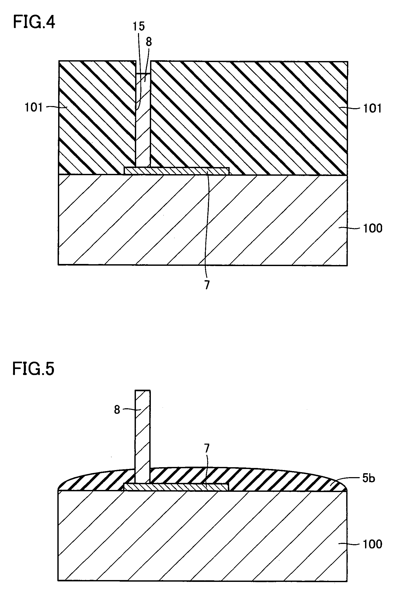
[0103]The semiconductor device according to this embodiment has a structure similar to that of the semiconductor device according to the first embodiment. The structure of the semiconductor device of this embodiment is different from that of the first embodiment in that, a groove 130 is formed in place of hole 13. That is, groove 130 is formed in insulation film 3 and semiconductor substrate 1. Furthermore, in this embodiment, a plurality of columnar conductive portions 8 are provided so as to align in groove 130 in an extending direction of groove 130.

[0104]As is seen from FIGS. 20-25, according to the structure of the semiconductor device of this embodiment, not semiconductor substrate 1 but only insulation film 5 exists between columnar conductive portions 8. In other words, insulating materials 5a and 5b fill a portion between columnar conductive portions 8 inside ...


PUM


Abstract

With a fluid insulating material applied on a convex substrate and a fluid insulating material applied on a concave substrate, a columnar conductive portion of the convex substrate is inserted into a hole of the concave substrate. With this, a conductive portion and an internal interconnection are electrically connected with each other via a bump. Therefore, a semiconductor device having a through electrode which enables a size reduction, has high reliability and is easily formed even with a large aspect ratio, and a method of manufacturing the same are obtained.

Description

BACKGROUND OF THE INVENTION[0001]1. Field of the Invention[0002]The present invention relates to a semiconductor device having a through (penetrating) electrode for electrically connecting a semiconductor substrate to another semiconductor substrate, semiconductor device or equipment, and to a method of manufacturing the same.[0003]2. Description of the Background Art[0004]A semiconductor device having a through electrode extending from a front surface to a back surface of a semiconductor substrate has been conventionally used. A conventional semiconductor device is formed with a method as described below.[0005]In the method, a first hole for embedding a through electrode having a prescribed depth and an interconnection to be connected to the through electrode are first formed on a semiconductor substrate. Then, an insulation film is deposited to cover an inner peripheral surface of the first hole and the interconnection. Thereafter, a portion of the insulation film inside the first...

Claims


Application Information

Patent Timeline
Patent Type & Authority Patents(United States)
IPC IPC(8): H01L21/44
CPCH01L21/6835H01L21/76898H01L23/481H01L24/18H01L24/82H01L25/0657H01L25/50H01L2924/19043H01L2924/014H01L2924/3025H01L2221/6834H01L2221/68363H01L2224/1147H01L2224/16H01L2224/18H01L2225/06513H01L2225/06541H01L2924/01013H01L2924/01078H01L2924/01079H01L2924/01005H01L2924/01006H01L2924/01033H01L2924/01068H01L2924/30105H01L2924/00014H01L2924/3512H01L2924/00011H01L2224/0401H01L23/48
Inventor NEMOTO, YOSHIHIKO
Owner RENESAS ELECTRONICS CORP
Why Eureka
Try Eureka