Silicon germanium emitter

a technology of silicon germanium and emitter, which is applied in the manufacture of semiconductor/solid-state devices, semiconductor devices, electrical apparatus, etc., can solve the problems of limiting the ac performance of transistors, and achieve the effects of reducing the delay time of emitter, increasing the cut-off frequency (ft) and the maximum oscillation frequency (fmax)

Active Publication Date: 2007-11-13
TAIWAN SEMICON MFG CO LTD
View PDF8 Cites 4 Cited by
  • Summary
  • Abstract
  • Description
  • Claims
  • Application Information

AI Technical Summary

Benefits of technology

[0005]In view of the foregoing, disclosed herein is a hetero-junction bipolar transistor (HBT) that incorporates a silicon-germanium emitter layer with a graded germanium concentration profile in order to reduce the emitter delay time and, thereby, increase the cut-off frequency (fT) and the maximum oscillation frequency (fMAX).
[0009]During this deposition process, a pure silicon buffer layer can first be deposited onto the collector layer. Then, germanium can be introduced into a lower portion of the silicon layer. Specifically, germanium can be introduced with a rapid ramp up in the germanium concentration (e.g., up to a maximum of approximately 40%). After the ramp up phase, the concentration of germanium introduced into the lower portion of the silicon layer can plateau for a period of time and then, begin a slow ramp down to approximately 0% germanium. Additionally, after the start and before the finish of the ramp down phase of introducing germanium into the lower portion of the silicon layer, a second conductivity type dopant (e.g., a p-type dopant, such as boron (B)) can simultaneously be introduced into this lower portion of the silicon layer. The deposition processes, described above, for the lower portion of the silicon layer effectively form the second conductivity type base layer (e.g., p-type base layer) of the HBT of the invention.

Problems solved by technology

In the near future emitter delay time may actually be of the same magnitude as base transmit times and may effectively limit the transistor AC performance.

Method used


Image

  • Silicon germanium emitter
  • Silicon germanium emitter
  • Silicon germanium emitter

Examples


Embodiment Construction

[0023]The present invention and the various features and advantageous details thereof are explained more fully with reference to the nonlimiting embodiments that are illustrated in the accompanying drawings and detailed in the following description. It should be noted that the features illustrated in the drawings are not necessarily drawn to scale. Descriptions of well-known components and processing techniques are omitted so as to not unnecessarily obscure the present invention. The examples used herein are intended merely to facilitate an understanding of ways in which the invention may be practiced and to further enable those of skill in the art to practice the invention. Accordingly, the examples should not be construed as limiting the scope of the invention.

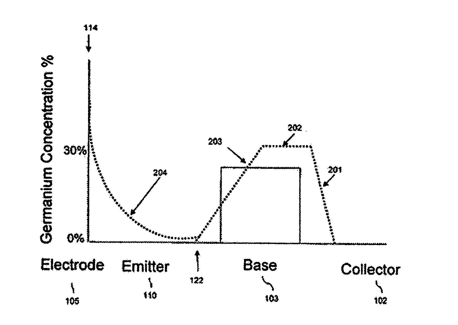
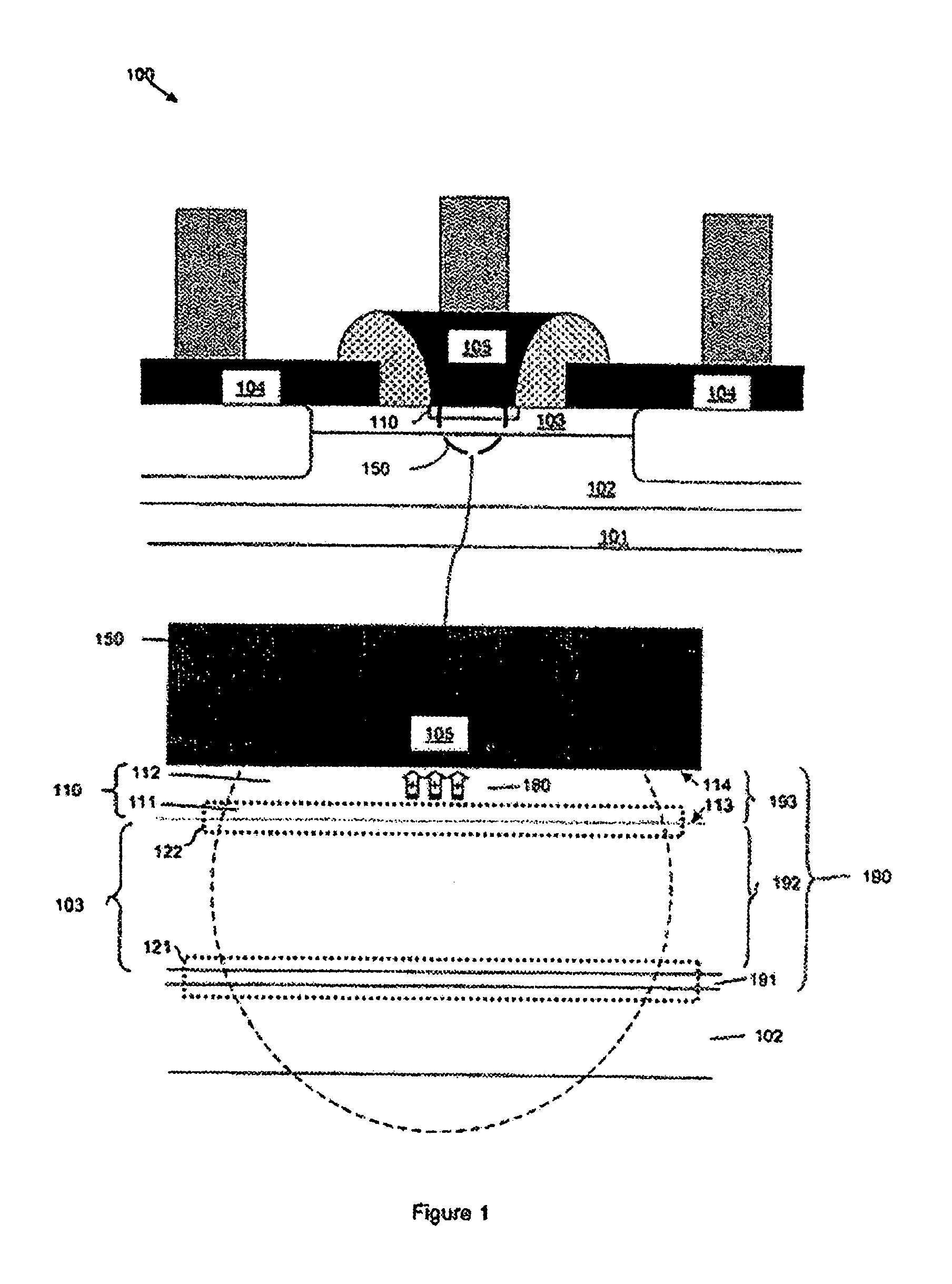
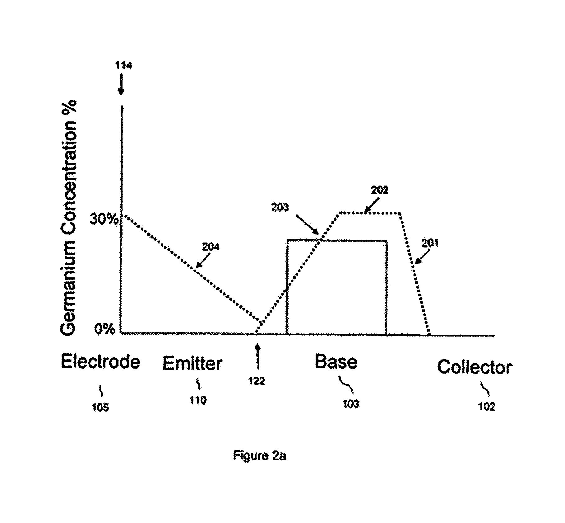
[0024]Referring to FIG. 1, disclosed is a hetero-junction bipolar transistor (HBT) structure 100. The structure 100 comprises two adjacent p-n junctions. Specifically, the HBT 100 comprises a first conductivity type collecto...


PUM


Abstract

Disclosed are an improved hetero-junction bipolar transistor (HBT) structure and a method of forming the structure that incorporates a silicon-germanium emitter layer with a graded germanium profile. The graded germanium concentration creates a quasi-drift field in the neutral region of the emitter layer. This quasi-drift field induces valence bandgap grading within the emitter layer so as to accelerate movement of holes from the base layer through the emitter layer. Accelerated movement of the holes from the base layer through the emitter layer reduces emitter delay time and thereby, increases the cut-off frequency (fT) and the maximum oscillation frequency (fMAX) of the resultant HBT.

Description

BACKGROUND OF THE INVENTION[0001]1. Field of the Invention[0002]The invention relates to hetero-junction bipolar transistors and, more particularly, to a hetero-junction bipolar transistor structure with an emitter that exhibits a reduced delay time and a method of forming the structure.[0003]2. Description of the Related Art[0004]As the switching speed of silicon germanium (SiGe) hetero-junction bipolar transistors (HBTs) approaches and extends beyond 350 GHz, the base transmit time for such HBT devices is in the range of approximately 100 fs. The emitter delay time for such devices is typically smaller than the base transmit time. However, as base size is scaled down, the emitter transmit time is becoming an increasing portion of the overall HBT forward transmit time. In the near future emitter delay time may actually be of the same magnitude as base transmit times and may effectively limit the transistor AC performance. Thus, there is a need in the art for a SiGe HBT that exhibit...

Claims


Application Information

Patent Timeline
Patent Type & Authority Patents(United States)
IPC IPC(8): H01L29/739H01L31/00
CPCH01L29/7378H01L29/66318
Inventor PAGETTE, FRANCOIS
Owner TAIWAN SEMICON MFG CO LTD
Why Eureka
Try Eureka