Stacked piezoelectric element and method of fabrication thereof

a piezoelectric element and stacking technology, applied in piezoelectric/electrostrictive/magnetostrictive devices, piezoelectric/electrostriction/magnetostriction machines, electrical devices, etc., can solve the problems of conduction failure, high possibility of above failure, and delaminate conductive adhesives from the side faces of ceramic stacks, so as to improve adhesion and enhance the anchoring effect. , the effect of not easily delamina

Inactive Publication Date: 2007-11-13
DENSO CORP
View PDF15 Cites 7 Cited by
  • Summary
  • Abstract
  • Description
  • Claims
  • Application Information

AI Technical Summary

Benefits of technology

[0016]That is, by forming the electrode recess as described above, not only is the end face of the internal electrode layer exposed in the side face of the ceramic stack, but also a portion of the surface of the internal electrode layer is exposed inside the electrode recess. As a result, the applied conductive adhesive is in contact with the internal electrode layer not only in the side face but also in the electrode recess. In this way, the contact area between the conductive adhesive and the internal electrode layer is increased compared with that in the prior known structure, ensuring reliable conductance between the internal electrode layer and the conductive adhesive.
[0031]As described above, according to this invention, a fabrication method can be provided for fabricating a stacked piezoelectric element that has excellent durability and reliability by ensuring reliable electrical conduction between the internal electrode layer and the conductive adhesive.

Problems solved by technology

There has therefore been the problem that the conductive adhesive may delaminate from the side face of the ceramic stack due to the stress, etc., caused by the deformation of the piezoelectric layer during operation.
This has led to the possibility of a contact failure occurring between the internal electrode layer and the conductive adhesive, resulting in conduction failure.
Furthermore, as the area of the end face of the internal electrode layer exposed in the side face of the ceramic stack is small, the possibility of the above failure dramatically increases in the event of delamination of the conductive adhesive.
This method, however, involves manufacturing problems such as a difficult in quality control during volume production and the need for masking portions where shot blasting is not to be applied.
However, with any of the above methods, the area of the end face of the internal electrode is nevertheless small, and there still exists the possibility that the conductive adhesive may delaminate, because the adhesive deteriorates and the adhesion drops as the piezoelectric layer is repeatedly stressed due to deformation and heat expansion during driving.
Accordingly, it is difficult to solve the conduction failure problem.

Method used


Image

  • Stacked piezoelectric element and method of fabrication thereof
  • Stacked piezoelectric element and method of fabrication thereof
  • Stacked piezoelectric element and method of fabrication thereof

Examples


example

Example 1

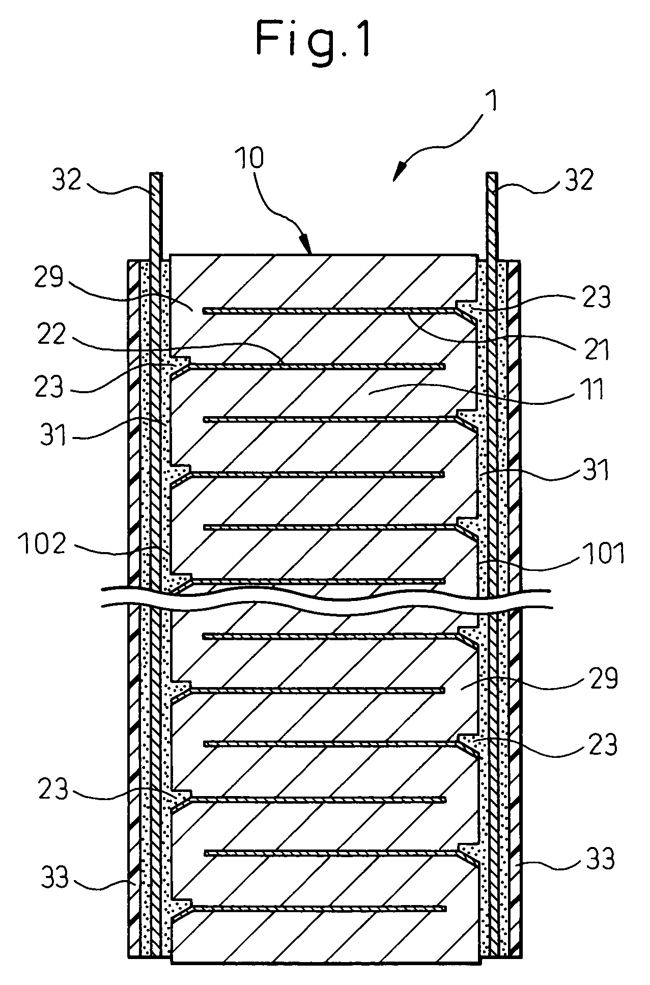
[0069]A stacked piezoelectric element and a method of fabrication thereof according to an example of the present invention will be described with reference to FIGS. 1 to 14.

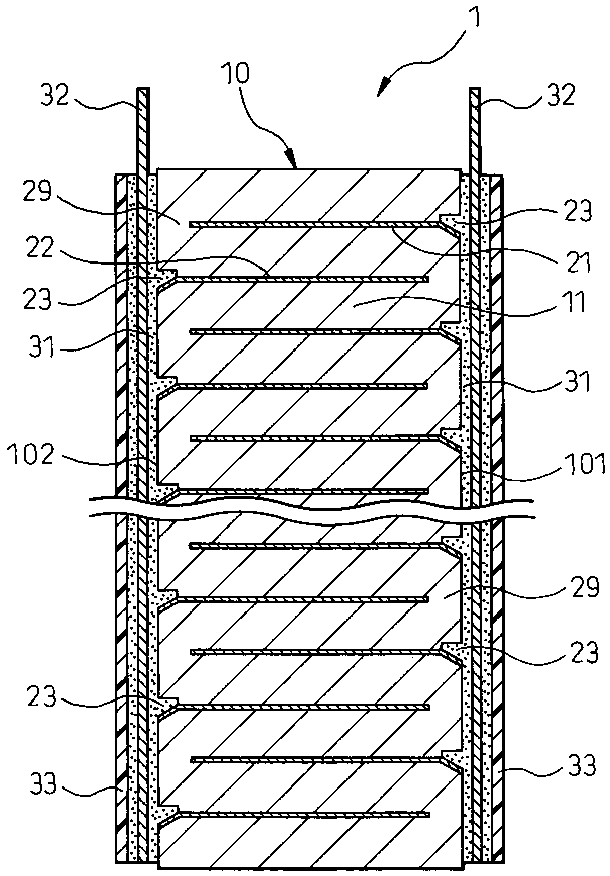
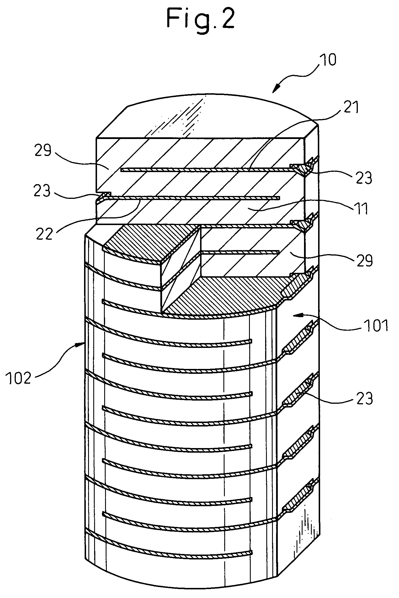
[0070]As shown in FIGS. 1 and 2, the stacked piezoelectric element 1 according to this embodiment comprises: a ceramic stack 10 constructed by alternately stacking piezoelectric layers 11 made of a piezoelectric material and internal electrode layers 21, 22 having electrical conductivity; and external electrodes 32 bonded to the side faces 101 and 102 of the ceramic stack 10 via an electrically conductive adhesive 31.

[0071]The side faces 101 and 102 of the ceramic stack 10 are provided with electrode recesses 23 each formed by indenting a portion of the edge of each of the internal electrode layers 21, 22 in the stacking direction thereof thereby forming a gap between it and the overlying piezoelectric layer 11, and the conductive adhesive 31 is applied so as to enter the electrode recesses 23 from the s...

example 2

[0125]This example differs from the stacked piezoelectric element 1 of Example 1 in that slits 12 are formed in the outer circumferential surface of the ceramic stack 10, as shown in FIG. 18.

[0126]In the fabrication method of the stacked piezoelectric element 1 of this example, dissipating slit layers 120 which are subsequently caused to dissipate in the calcining step are printed on the green sheet 110 in the printing step and, adjacent to the dissipating slit layers 120, a spacer layer 111 that is to be left after calcining is printed to the same thickness as the dissipating slit layers 120.

[0127]Then, in the intermediate stack forming step, electrode-containing pieces 51, each comprising the electrode material 200 applied on the green sheet 110 and the recessed portion 230 formed thereon, and dissipating-slit-layer-containing pieces 52, each comprising the dissipating slit layers 120 and the spacer layers 111 formed on the green sheet 110, are fabricated and stacked together.

[012...

example 3

[0140]This example is based on the ceramic stack 10 of Example 1, but the shapes and positions of the internal electrode layers 21, 22 and the slits 12 are changed in various ways. These changes will be described in detail with reference to FIGS. 18 to 22 which include drawings showing the ceramic stack 10 of the second example.

[0141]The shape and position of each of the internal electrode layers 21, 22 can be changed in the desired manner by changing the printing positions of the electrode material 200 and the spacer layer 111 to be printed within the punching area 41 on the green sheet 110 in the printing step.

[0142]Further, the shape and position of the slits 12 can be changed in the desired manner by changing the printing positions of the dissipating slit layers 120 and the spacer layer 111 to be printed within the punching area 41 on the green sheet 110 in the printing step or by changing the order in which the electrode-containing pieces 51 and the dissipating-slit-layer-conta...


PUM

PropertyMeasurementUnit
thicknessaaaaaaaaaa
temperatureaaaaaaaaaa

Abstract

This invention provides a stacked piezoelectric element that has excellent durability and reliability by ensuring reliable electrical conduction between internal electrode layer and conductive adhesive, and a method of fabricating such a stacked piezoelectric element, wherein the stacked piezoelectric element 1 comprises: a ceramic stack 10 constructed by alternately stacking piezoelectric layers 11 made of a piezoelectric material and internal electrode layers 21, 22 having electrical conductivity; and external electrodes 32 bonded to the side faces 101 and 102 of the ceramic stack 10 via an electrically conductive adhesive 31. The side faces 101 and 102 of the ceramic stack 10 are provided with electrode recesses 23 each formed by indenting a portion of the edge of each of the internal electrode layers 21, 22 in the stacking direction thereof thereby forming a gap between it and the overlying piezoelectric layer 11, and the conductive adhesive 31 is applied so as to enter the electrode recesses 23 from the side faces 101 and 102 of the ceramic stack 10.

Description

[0001]This application is a new U.S. patent application that claims benefit of JP 2004-374466, filed 24 Dec. 2004, the entire contents of which being herein incorporated by reference.FIELD OF THE INVENTION[0002]The present invention relates to a stacked piezoelectric element, adapted for use as a piezoelectric actuator or the like, and a method of fabrication thereof.BACKGROUND OF THE INVENTION[0003]In recent years, the development of automotive fuel injectors, etc., that use stacked piezoelectric elements as piezoelectric actuators has been proceeding to address automotive environmental problems and other automotive related issues such as fuel economy and exhaust emissions.[0004]A stacked piezoelectric element generally comprises: a ceramic stack constructed by alternately stacking a piezoelectric layer made of a piezoelectric material and an internal electrode layer (or internal electrode) having electrical conductivity; and an external electrode bonded to a side face of the ceram...

Claims


Application Information

Patent Timeline
Patent Type & Authority Patents(United States)
IPC IPC(8): H01L41/083H01L41/047H01L41/187H01L41/22H01L41/273H01L41/293H01L41/297H01L41/339
CPCH01L41/0472H01L41/273H01L41/293H01L41/083H01L41/0471H01L41/297H10N30/871H10N30/872H10N30/503H10N30/053H10N30/063H10N30/067
Inventor IWASE, AKIOKADOTANI, SHIGEITOU, TETSUJI
Owner DENSO CORP
Why Eureka
Try Eureka