Methods and apparatus for inspecting a sample

a sample and apparatus technology, applied in the field of apparatus and methods for sampling, can solve the problems of high complexity of semiconductor manufacturing, device failure, and partial blockage of beams, and achieve the effect of enhancing contras

Active Publication Date: 2007-11-13
KLA TENCOR TECH CORP
View PDF4 Cites 75 Cited by
  • Summary
  • Abstract
  • Description
  • Claims
  • Application Information

AI Technical Summary

Benefits of technology

[0008]Accordingly, the present invention provides methods and apparatus for inspecting or imaging a sample, such as a semiconductor wafer or reticle. In general, an optical inspection or microscopy tool that has a complex Fourier filter which is positioned in the Fourier plane of the radiation beam output from the sample in response to an incident beam striking the sample is provided. Use of such Fourier filter is also disclosed. In one implementation, the complex Fourier is designed to alter a phase of the scattered spatial portions of the output beam relative to the specular spatial portions of the output beam so as to enhance the contrast between the two. In a further implementation, the Fourier filter is designed to alter both a phase and an amplitude of the scattered spatial portions of the output beam so as to contrast with the specular spatial portions of the output beam. In another implementation, the complex Fourier filter serves to eliminate the effects of repeating structures on the sample from the output beam. The complex Fourier filter is used in conjunction with a complementary illumination aperture.
[0009]In one embodiment, an apparatus for inspecting or imaging a semiconductor sample is disclosed. The apparatus generally includes an illumination lens arrangement for directing an incident beam towards a sample and an illumination aperture that includes at least a first area and a second area. The first area is arranged to block a blocked spatial portion of the incident beam and the second area is arranged to transmit a transmitted spatial portion of the incident beam towards the sample. The apparatus also includes an output lens arrangement for directing an output beam from the sample towards a detector, the output beam comprising a specular portion and a scattered light portion and a complex Fourier filter positioned within a Fourier plane of the sample. The complex Fourier filter has at least a first area and a second area that vary in material composition and / or thickness, and the relative material compositions and thickness of the first and second area are selected so as to alter a phase of the specular portions of the output beam relative to the scattered portions of the output beam so as to enhance contrast between the scattered and specular light portions of the output beam. In a further aspect, the relative material compositions and thickness of the first and second area are further selected so as to alter an amplitude (in addition to the phase) of the specular portions of the output beam relative to the scattered portions of the output beam so as to enhance contrast between the scattered and specular light portions of the output beam.
[0011]In a specific implementation, the first area of the complex Fourier filter is formed from a transparent substrate having a first thickness and the second area of the complex Fourier filter is formed from a thin film and the transparent substrate. The second area has a second thickness which differs from the first thickness. In a particular embodiment, the first area of the complex Fourier filter is formed from a step in the transparent substrate. In one aspect, the step height is also selected so as to alter a phase of the specular portions of the output beam relative to the scattered portions of the output beam so as to enhance contrast between the scattered and specular light portions of the output beam.
[0018]In one aspect, the output beam is transmitted through the sample. In another aspect, the output beam is both reflected from and transmitted through the sample. In yet another aspect, the output beam is both reflected and scattered from the sample. In a specific implementation, the illumination aperture is in the form of a plurality of illumination sources which are configurable to be selectively directed onto a first plurality of ends of a plurality optical fibers that are arranged to output the incident beam in the form of a plurality of incident beams from a second plurality of ends of the fibers. The fibers are coupled with a fiber modulator which is operable to substantially eliminate the speckle noise of the incident beams. In another aspect, the illumination lens arrangement and the output lens arrangement are both movable so as to adjust the complex Fourier filter dimensions.

Problems solved by technology

Generally, the industry of semiconductor manufacturing involves highly complex techniques for fabricating integrating circuits using semiconductor materials.
Due to the large scale of circuit integration and the decreasing size of semiconductor devices, decreasingly small defects, such as a particle, can cause the devices to fail.
That is, portions of the beam are totally blocked by the mask, while other portions of the beam pass unimpeded through the mask.
Although these mask or aperture techniques have proved to be effective in many applications, they have limited sensitivity enhancement with respect to low contrast structures on the wafer, such as high aspect ratio vias.

Method used


Image

  • Methods and apparatus for inspecting a sample
  • Methods and apparatus for inspecting a sample
  • Methods and apparatus for inspecting a sample

Examples


Embodiment Construction

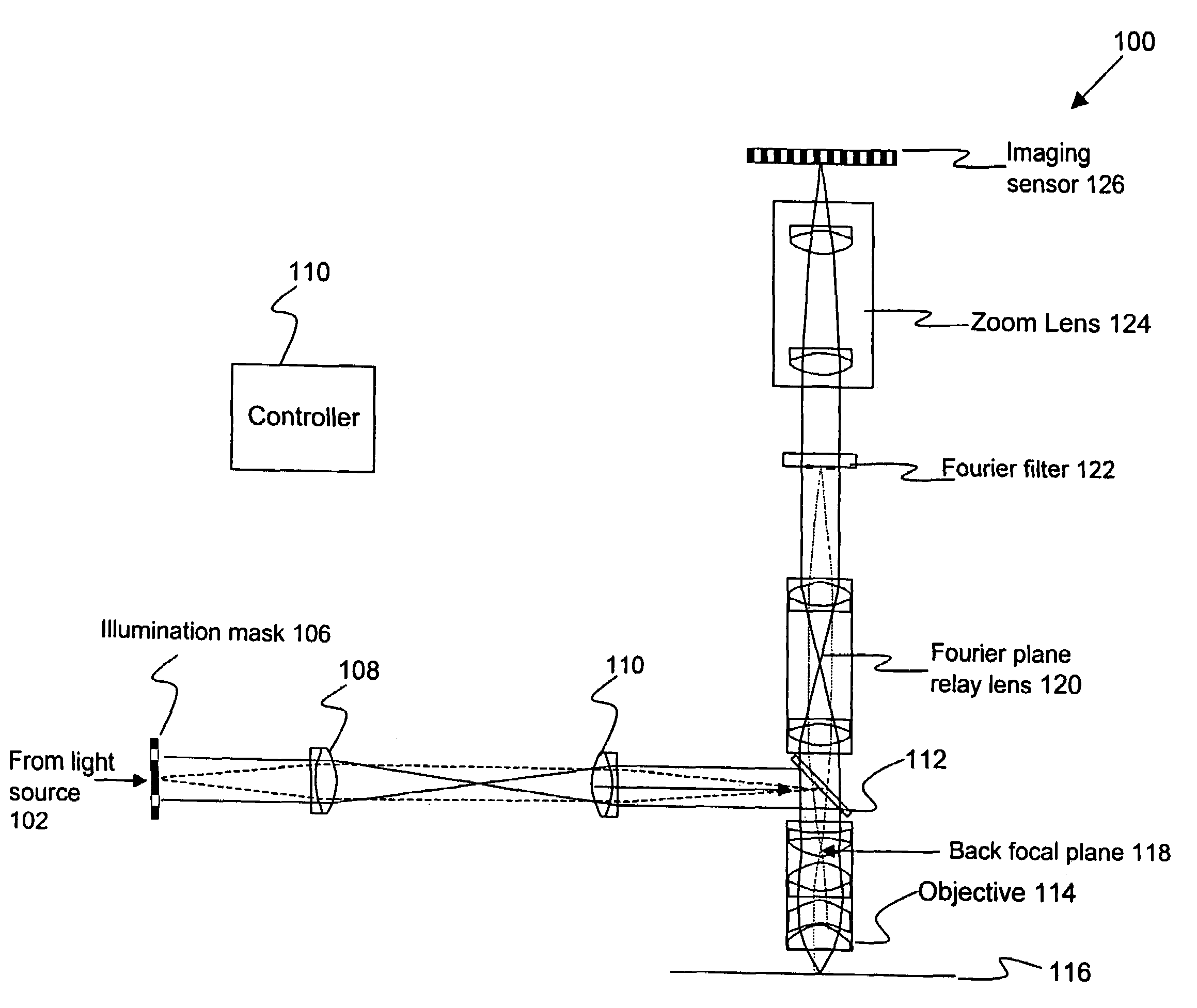
[0033]Reference will now be made in detail to a specific embodiment of the invention. An example of this embodiment is illustrated in the accompanying drawings. While the invention will be described in conjunction with this specific embodiment, it will be understood that it is not intended to limit the invention to one embodiment. On the contrary, it is intended to cover alternatives, modifications, and equivalents as may be included within the spirit and scope of the invention as defined by the appended claims. In the following description, numerous specific details are set forth in order to provide a thorough understanding of the present invention. The present invention may be practiced without some or all of these specific details. In other instances, well known process operations have not been described in detail in order not to unnecessarily obscure the present invention.

[0034]Low contrast defects and their surrounding area tend to have a slightly different refractive index tha...


PUM

PropertyMeasurementUnit
light emission wavelengthaaaaaaaaaa
thicknessaaaaaaaaaa
areaaaaaaaaaaa

Abstract

Disclosed are methods and apparatus for inspecting or imaging a sample, such as a semiconductor wafer or reticle. In general, an optical inspection or microscopy tool that has a complex Fourier filter positioned in the Fourier plane of the radiation beam output from the sample in response to an incident beam striking the sample is provided. Use of such Fourier filter is also disclosed. In one implementation, the complex Fourier is designed to alter a phase, and possibly amplitude, of the scattered spatial portions of the output beam relative to the specular spatial portions of the output beam so as to enhance the contrast between the two. In another implementation, the complex Fourier serves to filter the effects of repeating structures on the sample from the output beam. The complex Fourier filter is used in conjunction with a complementary illumination aperture.

Description

CROSS REFERENCE TO RELATED PATENT APPLICATION[0001]This application claims priority of U.S. Provisional Patent Application No. 60 / 556,607, entitled METHODS AND APPARATUS FOR INSPECTING A SAMPLE, filed 25 Mar. 2004 by Mehdi Vaez-Iravani, et al., which application is incorporated herein by reference in its entirety for all purposes.BACKGROUND OF THE INVENTION[0002]This invention pertains to apparatus and methods for inspecting a sample, such as a semiconductor wafer or photomask, using an optical inspection system. It also pertains to apparatus and methods for enhancing the detection of defects in such optical inspection systems.[0003]Generally, the industry of semiconductor manufacturing involves highly complex techniques for fabricating integrating circuits using semiconductor materials. Due to the large scale of circuit integration and the decreasing size of semiconductor devices, decreasingly small defects, such as a particle, can cause the devices to fail. Defect inspection proce...

Claims


Application Information

Patent Timeline
Patent Type & Authority Patents(United States)
IPC IPC(8): G01N21/00
CPCG01N21/95623G02B27/46G02B21/06
Inventor VAEZ-IRAVANI, MEHDIZHAO, GUOHENG
Owner KLA TENCOR TECH CORP
Why Eureka
Try Eureka