Method for reducing argon diffusion from high density plasma films

a plasma film and high density technology, applied in the field of forming semiconductor devices, can solve the problems of metal interconnect structures that cannot be used at the temperature, metal defects that get buried in ild films, and the inability to handle wiring requirements, etc., to reduce the number of metal defects, reduce the amount of metal defects, and reduce the content of die argon

Inactive Publication Date: 2007-11-20
TAIWAN SEMICON MFG CO LTD
View PDF8 Cites 44 Cited by
  • Summary
  • Abstract
  • Description
  • Claims
  • Application Information

AI Technical Summary

Benefits of technology

[0011]Another object of this invention is to describe a two-step HDP-CVD process to minimize die argon content in the top part of said gap filling inter level dielectric film in order to reduce metal defects.
[0012]In accordance with these objectives, a two-step HDP-CVD process is described wherein the argon content in the film is controlled by using two different argon concentrations in the argon / silane / oxygen gas mixture. The first step deposition uses high argon concentration and low sputter etch-to-deposition (E / D) ratio. In the second step, a lower argon concentration mid lower E / D ratio are used. By controlling argon concentration in the top part of the film to a low value, a reduced number of metal defects are achieved.

Problems solved by technology

With the increase in the number of transistors on a given silicon chip, the metal interconnect structures also are becoming dense to handle the wiring requirement for these integrated circuits (IC).
Although chemical vapor deposition (CVD) methods are suitable if filling high aspect ratio (height:gap-width) gaps have been used, they require higher temperatures>600 C. Such temperatures cannot be used since the metal wiring such as Aluminum, AlCu alloys have melting points close to these temperatures.
These methods therefore give rise to stresses in the ILD limits causing defects in metal lines that get buried in ILD films.
The prior art patents do not disclose or discuss the defects caused by the incorporation of argon atoms in the dielectric film during HDP-CVD process.

Method used


Image

  • Method for reducing argon diffusion from high density plasma films
  • Method for reducing argon diffusion from high density plasma films
  • Method for reducing argon diffusion from high density plasma films

Examples


Embodiment Construction

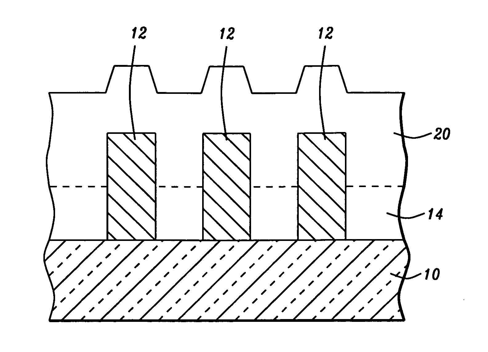
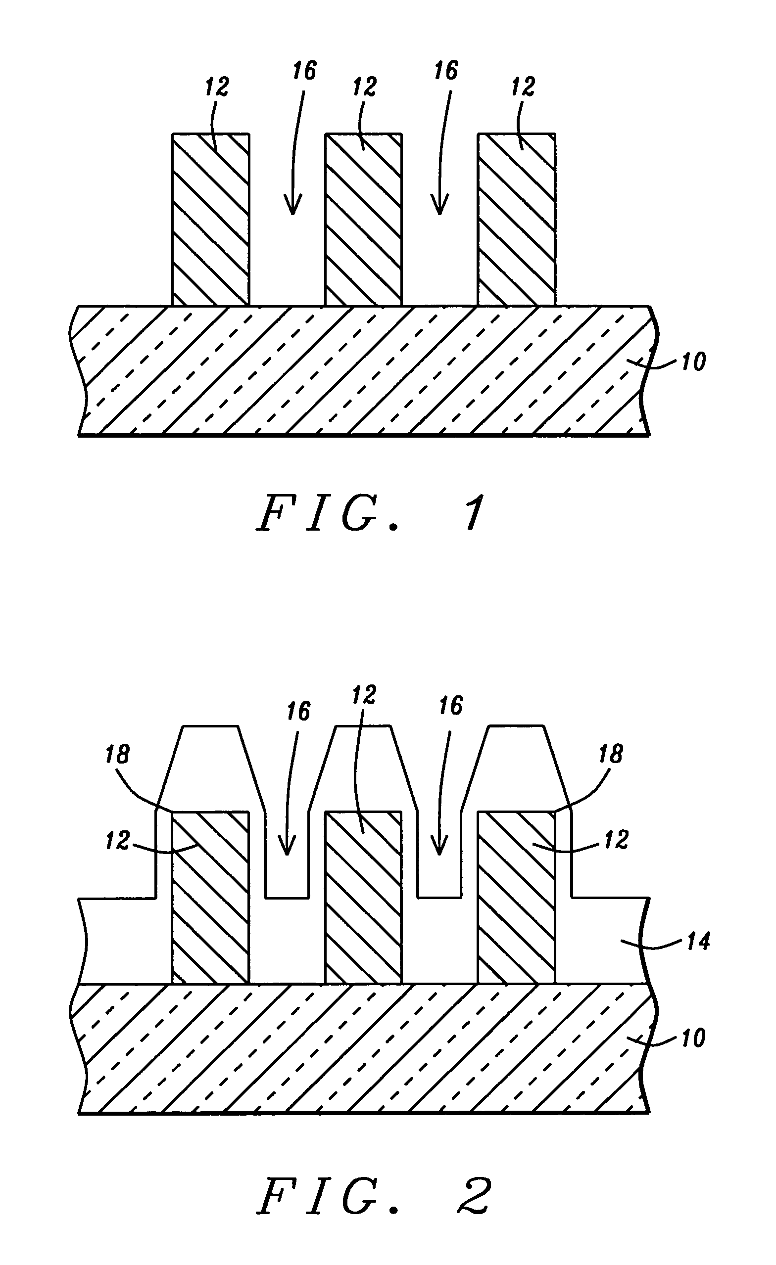
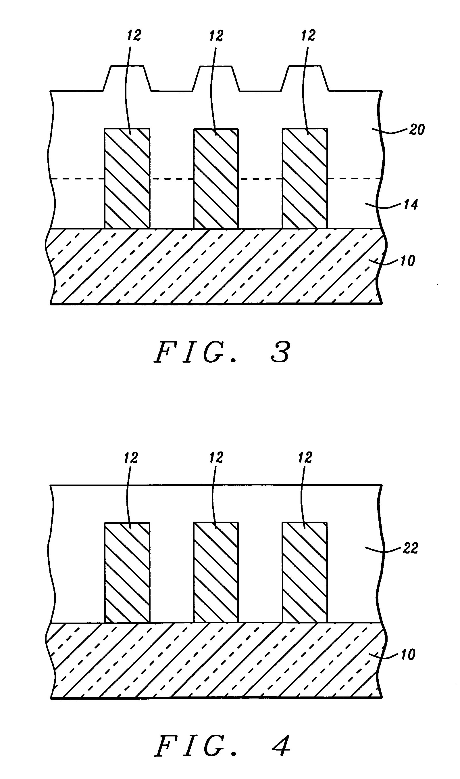
[0018]A first HDP-CVD inter level dielectric film 14 is then deposited, with the object of filling the gaps 16 between metal lines. HDP-CVD method is chosen since the film can be deposited at less than 400 C and the film quality is superior in terms gap-filling characteristics, density, and pinholes. Since the HDP-CVD is a plasma deposition method, it has both deposition and sputter etching components built-in. By controlling the ratio of sputter etching (E) and deposition (D) components, it is possible to tailor the properties of the films and gap-filling characteristics. For example, while filling high aspect ratio (height-to-gap width) gaps the openings of the gaps can get closed prematurely and produce large voids or key holes in the deposited film. By adjusting the etching component in the process, the gap openings can be kept open to achieve a more bottom-up filling. Too much of the etching component can result in metal line corner faceting since sputter etching can also erode...


PUM

PropertyMeasurementUnit
thicknessaaaaaaaaaa
concentrationaaaaaaaaaa
pressureaaaaaaaaaa

Abstract

A two-step high density plasma-CVD process is described wherein the argon content in the film is controlled by using two different argon concentrations in the argon / silane / oxygen gas mixture used for generating the high density plasma. The first step deposition uses high argon concentration and low sputter etch-to-deposition (E / D) ratio. High E / D ratio maintains the gap openings without necking. In the second step, a lower argon concentration and lower E / D ratio are used. Since observed metal defects are caused by argon diffusion in the top 200-300 nm of the HDP-CVD film, by controlling argon concentration in the top part of the film (i.e. second step deposition) to a low value, a reduced number of metal defects are achieved.

Description

FIELD OF THE INVENTION[0001]The present invention relates generally to a method of forming a semiconductor device, and more particularly to form defect-free metal interconnect structures with improved inter-level dielectric layers.DESCRIPTION OF THE PRIOR ART[0002]With the increase in the number of transistors on a given silicon chip, the metal interconnect structures also are becoming dense to handle the wiring requirement for these integrated circuits (IC). Chip size needs to be kept small to maintain the high speed of the IC device and to increase the number of dies per water. This is accomplished by distributing the wiring over several metal layers, the structure being usually known as multi level metal (MLM) layers. It is not uncommon to have upwards of six levels of metal layers with required number of interconnecting via between two successive metal layers.[0003]One conventional method of forming these MLM structures is deposit first level metal on a silicon water having devi...

Claims


Application Information

Patent Timeline
Patent Type & Authority Patents(United States)
IPC IPC(8): H01L21/31
CPCC23C16/045C23C16/401C23C16/45523H01L21/02164H01L21/76837H01L21/31612H01L21/31629H01L21/76801H01L21/02274
Inventor XIE, JUNYAP, HOON LIANYEAP, CHUIN BOONLOK, WEOI SAN
Owner TAIWAN SEMICON MFG CO LTD
Why Eureka
Try Eureka