
Electron source and an image display device including the electron source

Inactive Publication Date: 2007-11-20
CANON KK
View PDF20 Cites 8 Cited by
  • Summary
  • Abstract
  • Description
  • Claims
  • Application Information

AI Technical Summary

Benefits of technology

[0015]It is an object of the present invention to provide precursor to an electron source which has a capability for extending the life of an image display device by preventing (or at least substantially minimizing) 1) a degradation in a degree of vacuum provided in an image display apparatus, 2) a short circuit between adjacent wire electrodes via a getter, and 3) a degradation in the performance characteristics of the electron source, even when used for a long period of time, and also to provide an electron source and an image display device using the precursor.

Problems solved by technology

Cracks are generated at locally destructed, deformed or altered portions of the conductive film.
This is because if a gas is generated within the envelope to increase the pressure within the envelope, the gas adversely influences the electron source to reduce the amount of electron emission although the degree of the influence depends on the type of the gas, and it becomes impossible to display a bright image.
In some cases, the generated gas is ionized by the electron beam and damages the electron source due to the collision of the ionized gas with the electron source by being accelerated by an electron field for accelerating electrons.
First, the above-described coated layer formed on the substrate for forming an electron source may cause difficulty in maintaining the high-vacuum state within the envelope formed by connecting the substrate and the faceplate via the supporting frame, depending on the state of formation of the coated layer. It is estimated that this is because the inside of the coated layer may have gas permeability.
Second, the getter provided on the coated layer within the envelope in order to maintain a vacuum within the envelope may cause a short circuit between adjacent wire electrodes, even if the coated layer is made of an insulator. It is estimated that this is because a large number of bubbles are sometimes formed in the coated layer depending on the state of formation of the coated layer, and the bubbles are burst during heating at a high temperature to provide a state in which the wire electrodes are exposed. This short circuit may greatly degrade the quality of the formed image. Hence, in the worst case, the production yield of the image display device is degraded by manufacturing failed products.

Method used


Image

  • Electron source and an image display device including the electron source
  • Electron source and an image display device including the electron source
  • Electron source and an image display device including the electron source

Examples


Embodiment Construction

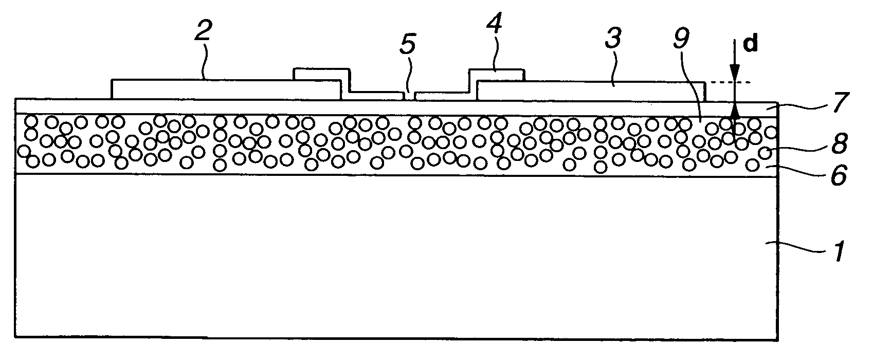
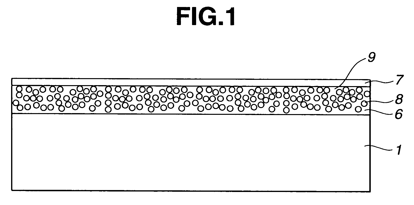
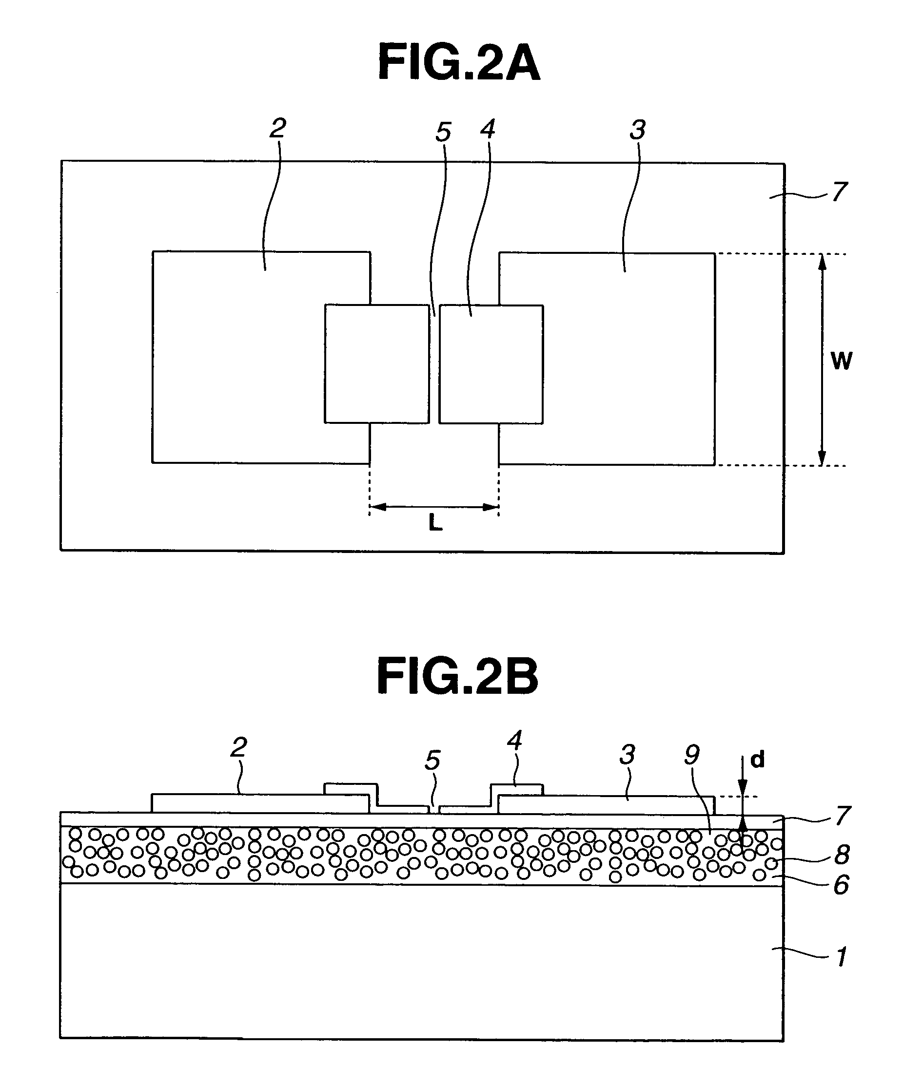
[0039]According to an aspect of the invention, a precursor to an electron source is provided. The electron source preferably is for being coupled to an image display member to form an image display apparatus, and the image display member is for displaying an image in response to being irradiated by electrons. According to one embodiment of the invention, the precursor is characterized in that it comprises a substrate, and an antistatic film provided on a surface of the substrate at a region where the electron emitting devices are to be disposed on the precursor to form the electron source. The antistatic film preferably is not provided on a region of that surface which is to be coupled to the image display member. Preferably, the antistatic film contains conductive particles.

[0040]According to another embodiment of the invention, a precursor to an electron source is provided, wherein the electron source is for being coupled to an image display member to form an image display apparat...


PUM


Abstract

A precursor to an electron source, having a capability for extending the life of an image display device by substantially preventing 1) a degradation in a degree of vacuum provided in an image display apparatus, 2) short-circuiting between adjacent wire electrodes via a getter, and 3) a degradation in performance characteristics of the electron source, even when used for a long time period. The electron source is for coupling to an image display member to form an image display apparatus, and the image display member is for displaying an image in response to being irradiated by electrons. The precursor preferably comprises a substrate, and an antistatic film provided on a surface of the substrate at a region where electron emitting devices are to be disposed on the precursor to form the electron source, but not on a region of that surface to be coupled to the image display member.

Description

BACKGROUND OF THE INVENTION[0001]1. Field of the Invention[0002]The present invention relates to a substrate for forming an electron source, an electron source using the substrate, and an image display device using the electron source.[0003]2. Description of the Related Art[0004]Two types of electron emitting devices, i.e., thermionic-cathode devices and cold-cathode devices, have been known. For example, surface-conduction-type devices, field-emission-type devices, metal / insulating layer / metal-type devices have been known as the cold-cathode devices.[0005]The surface-conduction-type devices utilize the phenomenon that electron emission occurs by causing a current to flow in a direction parallel to the surface of a small-area thin film formed on a substrate. In the surface-conduction-type devices, electron emitting portions are formed by performing current-supply processing, called current-supply forming, on a conductive film before performing electron emission. That is, the current...

Claims


Application Information

Patent Timeline
IPC IPC(8): H01J19/00H01J31/00H01J29/04H01J1/316H01J9/02H01J31/12
CPCH01J9/027H01J1/316
Inventor DANJO, KEISHIENOMOTO, TAKASHINUKANOBU, KOUKI
Owner CANON KK
Learn More