Polishing method for semiconductor wafer

a technology of polishing method and semiconductor wafer, which is applied in the direction of grinding machine components, manufacturing tools, lapping machines, etc., can solve the problems of generating a lot of a lot of minute projecting defects on the semiconductor wafer

Active Publication Date: 2007-12-04
SUMCO TECHXIV
View PDF15 Cites 6 Cited by
  • Summary
  • Abstract
  • Description
  • Claims
  • Application Information

AI Technical Summary

Benefits of technology

[0010]An object of the present invention is to provide a polishing method for a semiconductor wafer which provides proper polishing of the semiconductor wafer.

Problems solved by technology

However, when the system disclosed in the Document is applied to the rough polishing step, contaminants that are contained in the recycled polishing slurry and cannot be removed by filtering might cause a lot of minute projecting defects to be generated on the semiconductor wafer.
In addition, when the finishing-slurry prepared solution as described above is used in the finish polishing step, contaminants contained in the finishing-slurry prepared solution might cause a lot of projecting defects to be generated on the semiconductor wafer.

Method used


Image

  • Polishing method for semiconductor wafer
  • Polishing method for semiconductor wafer
  • Polishing method for semiconductor wafer

Examples


first embodiment

[0075]A first embodiment of the present invention will be described below with reference to the attached drawings.

[0076][Arrangement of Semiconductor Wafer Polishing Device]

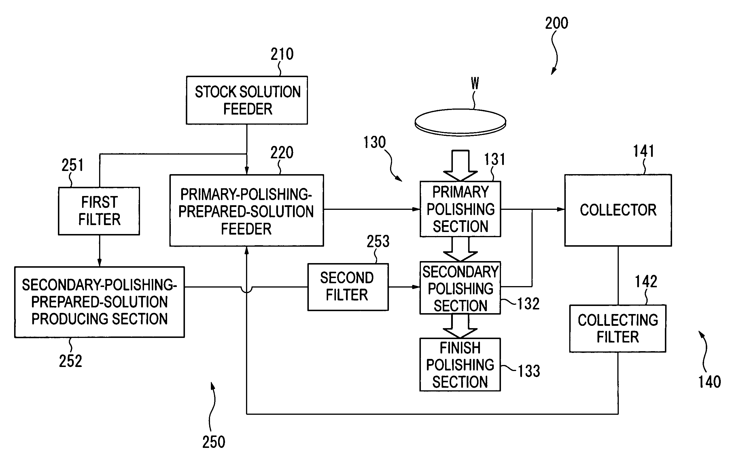
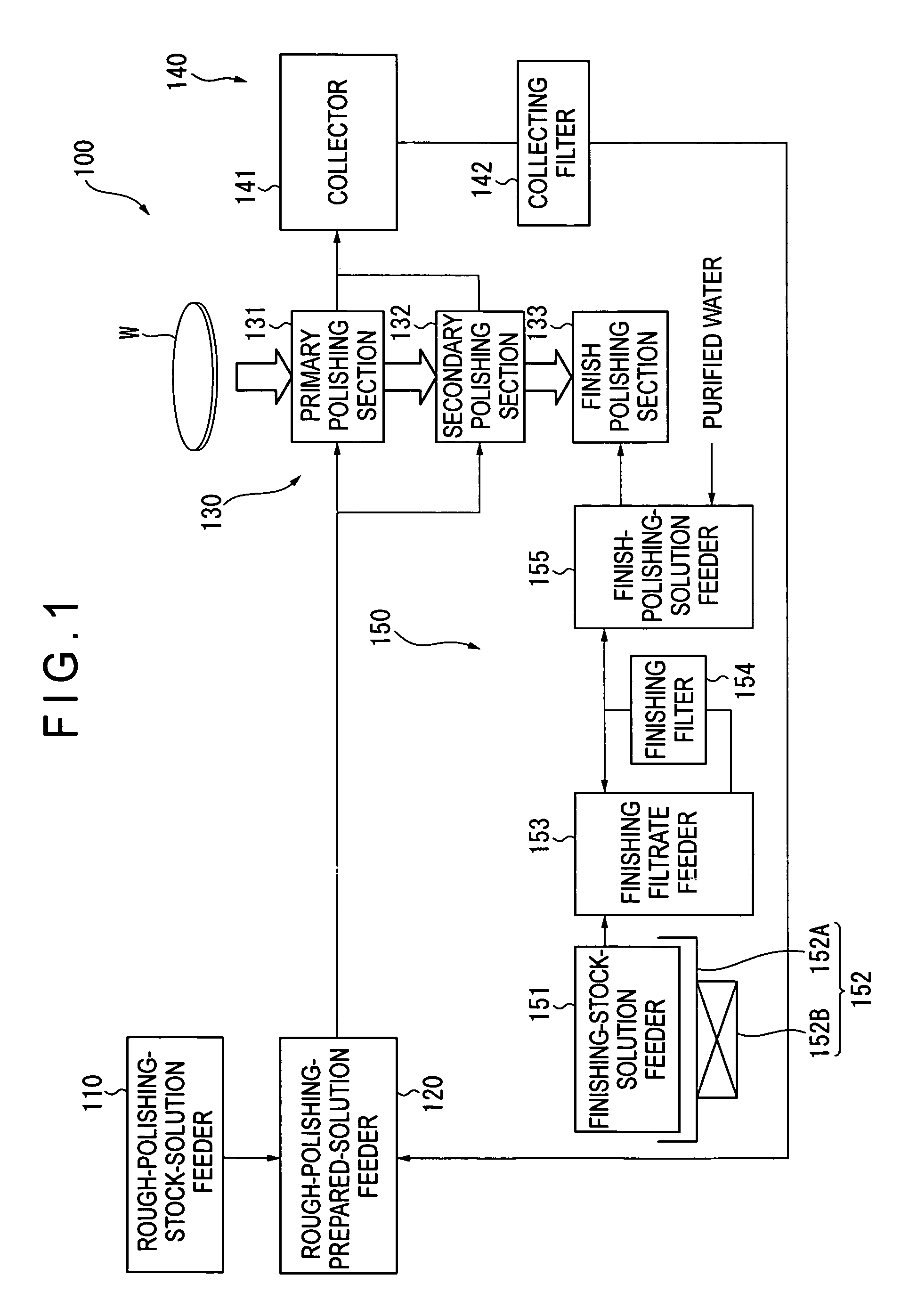
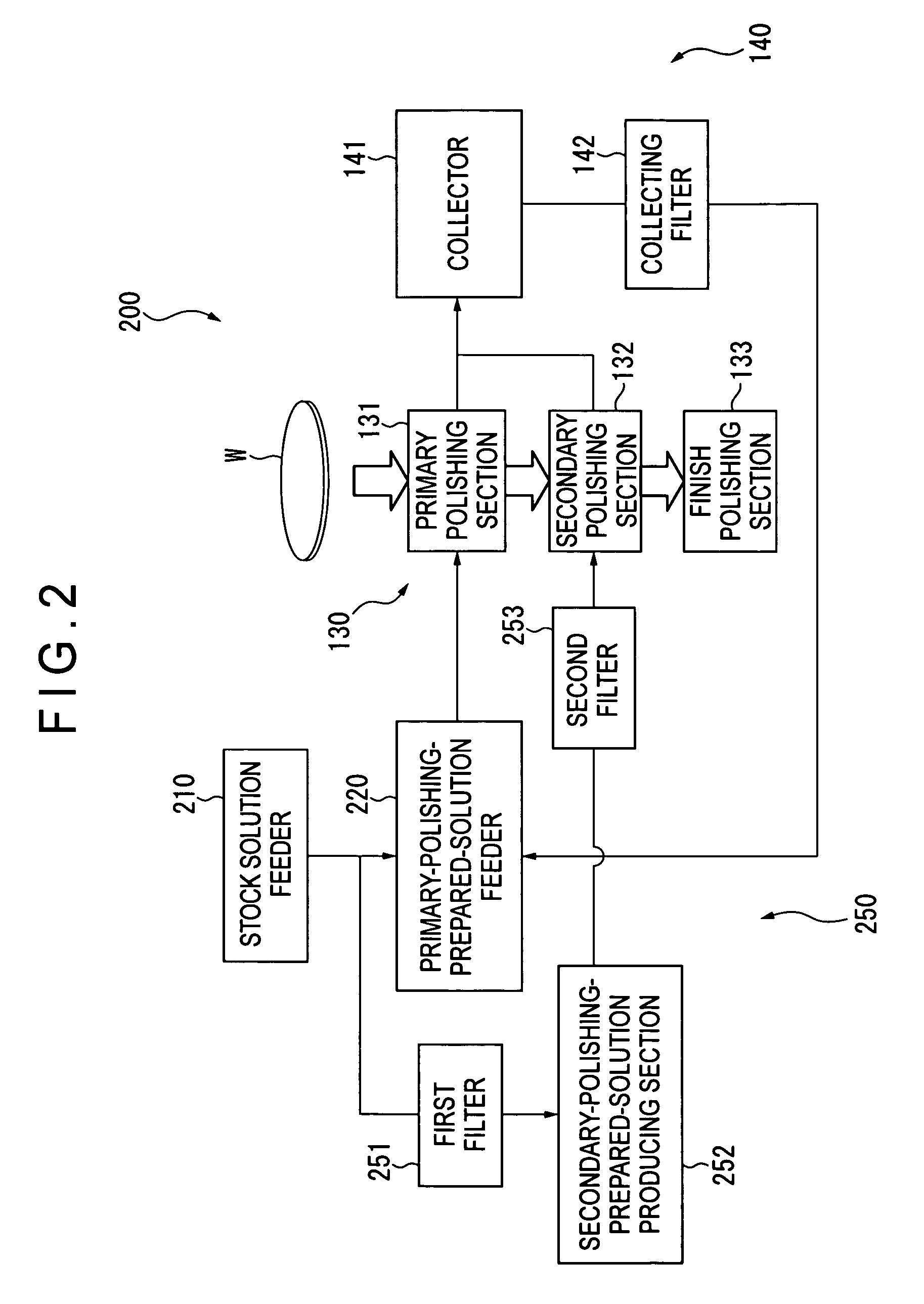
[0077]FIG. 1 is a block diagram showing an outline of a polishing device 100 of a semiconductor wafer W of the first embodiment.

[0078]The polishing device 100 polishes a surface of the semiconductor wafer W having the diameter of 200 mm through a plurality of steps using a polishing slurry containing silica particles. Specifically, the polishing device 100 polishes the semiconductor wafer W through primary polishing, secondary polishing and finish polishing. Incidentally, the polishing device 100 may polish a semiconductor wafer W having a diameter other than 200 mm.

[0079]As shown in FIG. 1, the polishing device 100 includes a rough-polishing-stock-solution feeder 110, a rough-polishing-prepared-solution feeder 120, a polishing section 130, a collecting section 140 and a slurry adjusting section 150.

[0080]In the ...

second embodiment

[0126]Now, the second embodiment of the present invention will be described below with reference to the attached drawings.

[0127]In the description below, the same reference numerals will be attached to the structures and components which are the same as the first embodiment to omit or simplify the detailed description thereof.

[0128][Arrangement of Semiconductor Wafer Polishing Device]

[0129]FIG. 2 is a block diagram showing an outline of a polishing device 200 of the semiconductor wafer W of the second embodiment.

[0130]A stock solution feeder 210 is made of, for instance, a PFA (tetrafluoroethylene-perfluoroalkylvinyl ether copolymer) and formed in a substantially box-like shape, the stock solution feeder 210 being connected to a primary-polishing-prepared-solution feeder 220 and a slurry adjusting section 250.

[0131]The stock solution feeder 210 is hermetically sealed and humidity of the internal space thereof is controlled to be 99% or higher. A rough-polishing-slurry stock solution...

third embodiment

[0200]Now, the third embodiment of the present invention will be described below with reference to the attached drawings.

[0201]In the description below, the same reference numerals will be attached to the structures and components which are the same as the first and second embodiments to omit or simplify the detailed description thereof.

[0202][Arrangement of Semiconductor Wafer Polishing Device]

[0203]FIG. 3 is a block diagram showing an outline of a polishing device 300 of the semiconductor wafer W of the third embodiment.

[0204]As shown in FIG. 3, the polishing device 300 includes a stock solution feeder 310, a primary-polishing-prepared-solution feeder 320, the polishing section 130, the collecting section 140 and a slurry adjusting section 350.

[0205]The stock solution feeder 310 is made of PFA and formed in, for instance, a substantially box-like shape, the stock solution feeder 310 connected to the primary-polishing-prepared-solution feeder 320.

[0206]The humidity of the internal ...


PUM

PropertyMeasurementUnit
particle sizeaaaaaaaaaa
energyaaaaaaaaaa
temperatureaaaaaaaaaa

Abstract

A polishing method includes a slurry adjusting step for adjusting a polishing slurry containing silica particles so that the number of silica particles having a composition ratio of Si / O of 50–60 wt % / 40–50 wt %, a modulus of elasticity of 1.4×10¹⁰ Pa or higher and a particle size of 1 μm or larger is 3000 pcs / ml or less. A semiconductor wafer is polished using the polishing slurry adjusted in the slurry adjusting step.

Description

BACKGROUND OF THE INVENTION[0001]1. Field of the Invention[0002]The present invention relates to a polishing method for a semiconductor wafer for polishing the semiconductor wafer.[0003]2. Description of Related Art[0004]As a method for polishing a semiconductor wafer using a polishing slurry, there has been conventionally employed a method including a primary polishing step, a secondary polishing step and a finish polishing step. In such polishing method, the polishing slurry is reused in the primary polishing step and the secondary polishing step in terms of production cost.[0005]As an arrangement applicable to such rough polishing steps prior to the finish polishing, there has been known a polishing system for polishing the semiconductor wafer using a recycled polishing slurry (see, for instance, Document: JP-A-2000-237959, left column of page 4 to right column of page 5).[0006]In a system disclosed in the Document, new slurry is fed from an unused slurry feeding unit to a buffer...

Claims


Application Information

Patent Timeline
Patent Type & Authority Patents(United States)
IPC IPC(8): B44C1/22H01L21/461
CPCB24B37/044B24B55/12H01L21/02024C09G1/02B24B57/04Y02P70/10
Inventor KOZASA, KAZUAKIYAMADA, MOTOHARUTOMITA, YASUHIROWAKABAYASHI, HIROMI
Owner SUMCO TECHXIV
Why Eureka
Try Eureka