Tunable optical filter with heater on a CTE-matched transparent substrate

Active Publication Date: 2007-12-04
II VI DELAWARE INC +1
View PDF72 Cites 37 Cited by
  • Summary
  • Abstract
  • Description
  • Claims
  • Application Information

AI Technical Summary

Problems solved by technology

These devices, which are made from amorphous semiconductor materials, exploit what had previously been viewed as an undesirable property of amorphous silicon, namely, its large thermo-optic coefficient.

Method used


Image

  • Tunable optical filter with heater on a CTE-matched transparent substrate
  • Tunable optical filter with heater on a CTE-matched transparent substrate
  • Tunable optical filter with heater on a CTE-matched transparent substrate

Examples


Embodiment Construction

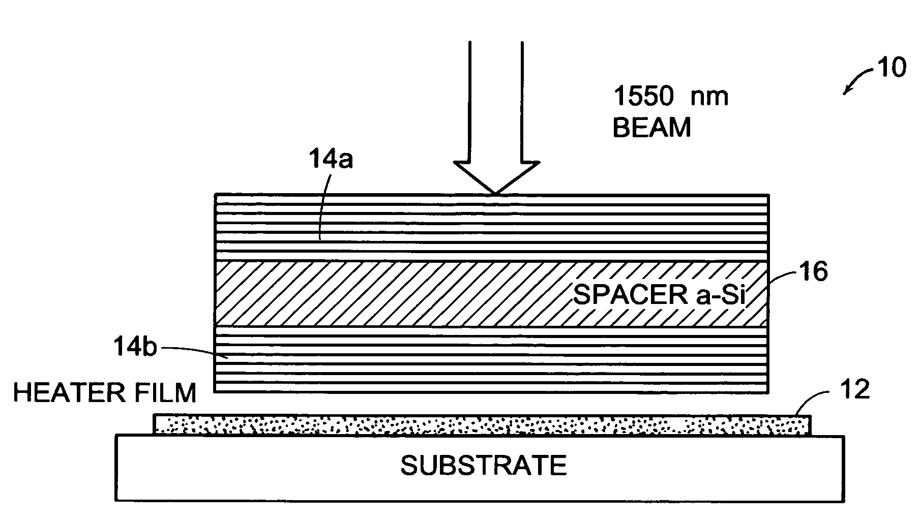
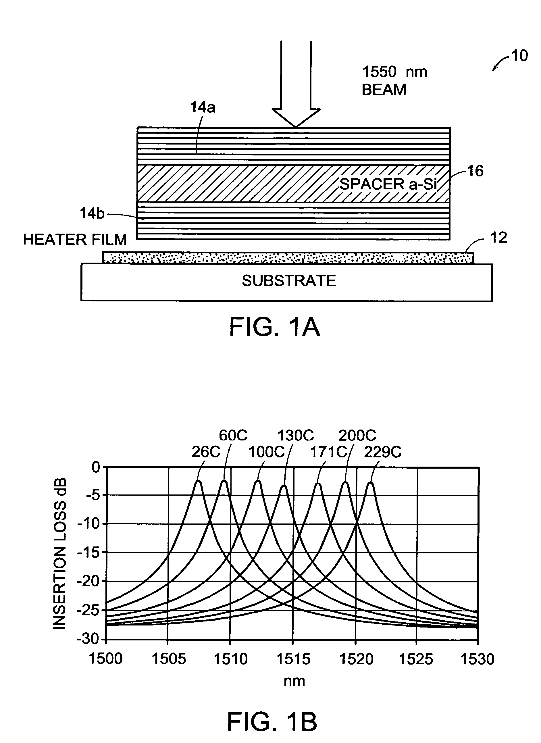
[0016]In general, a thermally tunable thin film optical filter is deposited directly on top of a doped single-crystal silicon sheet-resistive heater, which is in turn supported by a substrate that is transparent to the wavelength at which the optical filter is meant to operate. The substrate has a coefficient of thermal expansion (CTE) that is more closely matched to the CTE of the optical filter than is fused quartz silica that has been used in the past, thereby permitting the entire structure to expand and contract without experiencing excessive stress or resulting damaging when exposed to the large temperature excursions required for fabrication and for tuning. The method for fabricating this structure is as follows.

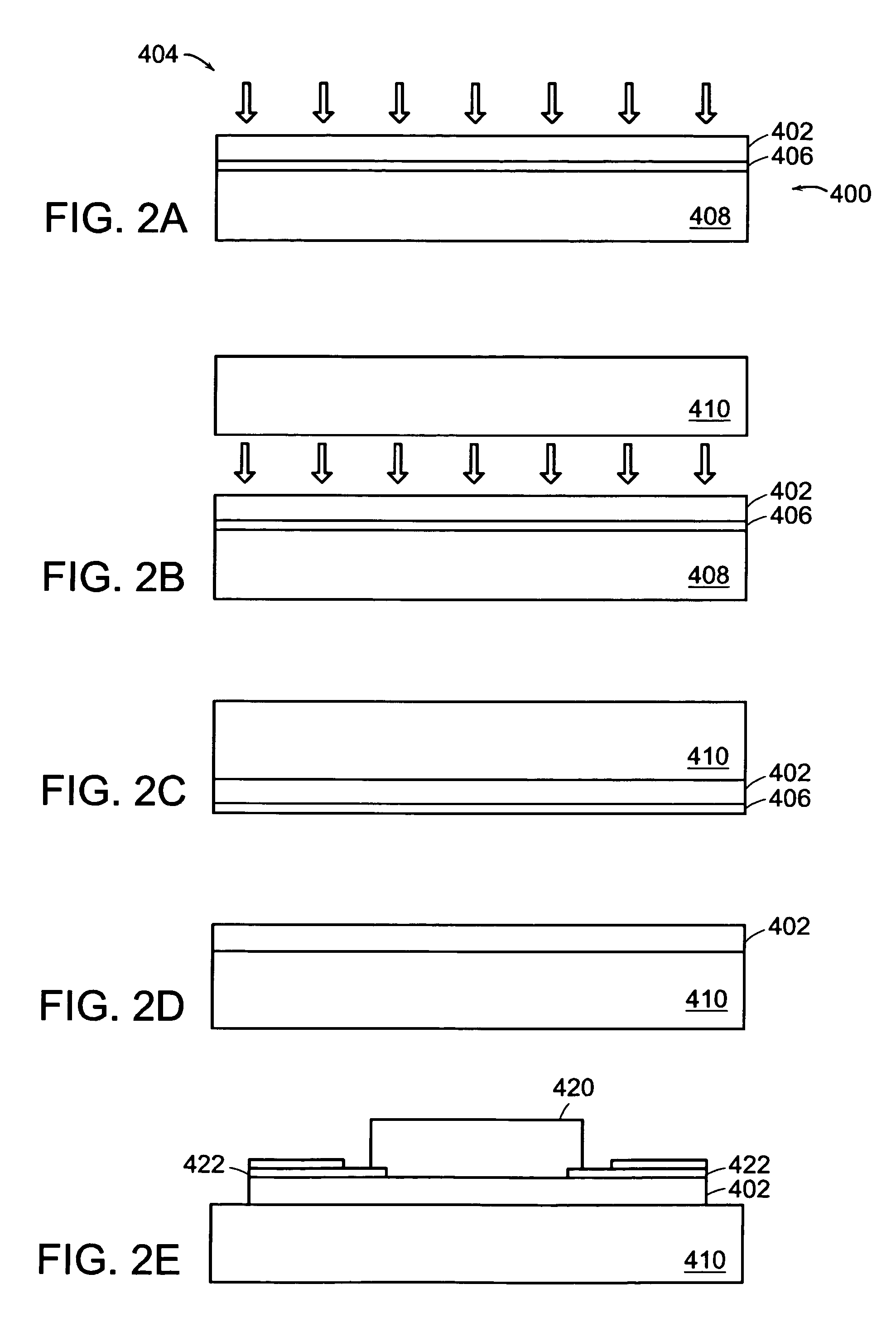
[0017]Referring to FIG. 2a-e, the process begins with an SOI wafer 400 that has a device layer 402 of the desired thickness. Device layer 402 is made of a high quality single-crystal silicon material and is bonded to an oxide layer (BOX layer) 406 that was formed on a...


PUM

PropertyMeasurementUnit
temperatureaaaaaaaaaa
thickaaaaaaaaaa
thickaaaaaaaaaa

Abstract

An optical device including: a glass substrate; a crystalline silicon layer bonded to the glass substrate; and a thermally tunable thin-film optical filter fabricated on top of the crystalline silicon layer.

Description

[0001]This application claims the benefit of U.S. Provisional Application No. 60 / 509,203, filed Oct. 7, 2003.TECHNICAL FIELD[0002]This invention generally relates to thermally tunable devices such as thermo-optically tunable thin film optical filters.BACKGROUND OF THE INVENTION[0003]There is a family of devices that are based on thermo-optically tunable, thin-film optical filters. These devices, which are made from amorphous semiconductor materials, exploit what had previously been viewed as an undesirable property of amorphous silicon, namely, its large thermo-optic coefficient. The performance of these devices is based on trying to maximize thermo-optic tunability in thin-film interference structures, instead of trying to minimize it as is often the objective for conventional fixed filters. The devices are characterized by a pass band centered at a wavelength that is controlled by the temperature of the device. In other words, by changing the temperature of the device one can shif...

Claims


Application Information

Patent Timeline
Patent Type & Authority Patents(United States)
IPC IPC(8): G02B27/00G02B5/28G02B6/34G02F1/01G02F1/21H01L21/00
CPCG02B5/285G02F1/218G02F1/21G02F1/0147
Inventor MA, EUGENE YI-SHANCOHEN, MITCHELL S.
Owner II VI DELAWARE INC
Why Eureka
Try Eureka