Method of multiple pulse laser annealing to activate ultra-shallow junctions

a laser annealing and ultra-shallow junction technology, applied in chemical vapor deposition coatings, electrical equipment, coatings, etc., can solve problems such as high source and drain series resistance, short channel effects become significant, and affect device performan

Active Publication Date: 2005-05-24
CHARTERED SEMICONDUCTOR MANUFACTURING
View PDF7 Cites 100 Cited by
  • Summary
  • Abstract
  • Description
  • Claims
  • Application Information

AI Technical Summary

Problems solved by technology

As device dimension continue to shrink, short channel effects become significant and begin to affect device performance.
As a consequence, the resultant lower impurity concentrations cause undesirably high source and drain series resistance.
The laser energy is not sufficient to melt and cause dopant infusion into the source / drain regions.

Method used


Image

  • Method of multiple pulse laser annealing to activate ultra-shallow junctions
  • Method of multiple pulse laser annealing to activate ultra-shallow junctions
  • Method of multiple pulse laser annealing to activate ultra-shallow junctions

Examples


Embodiment Construction

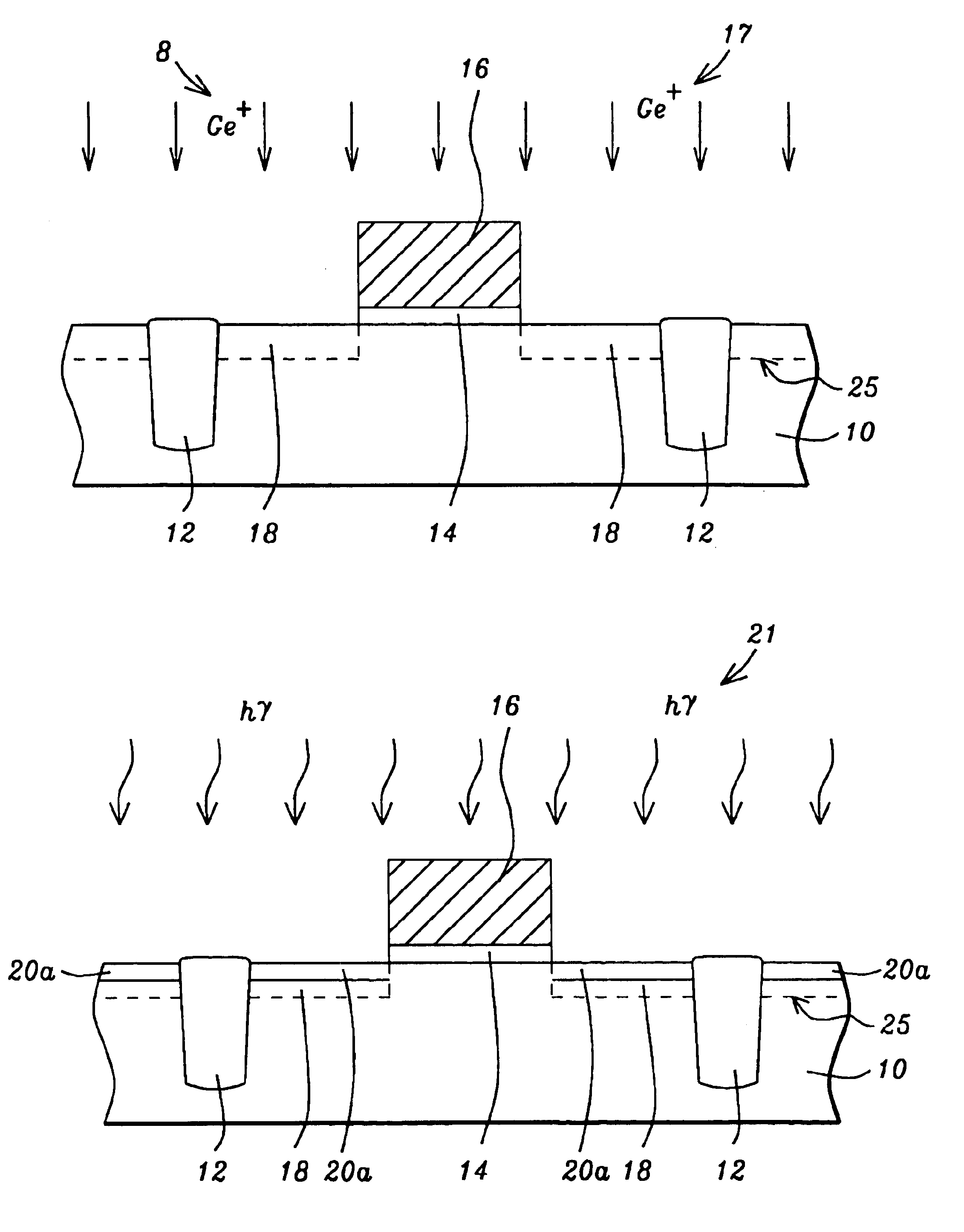
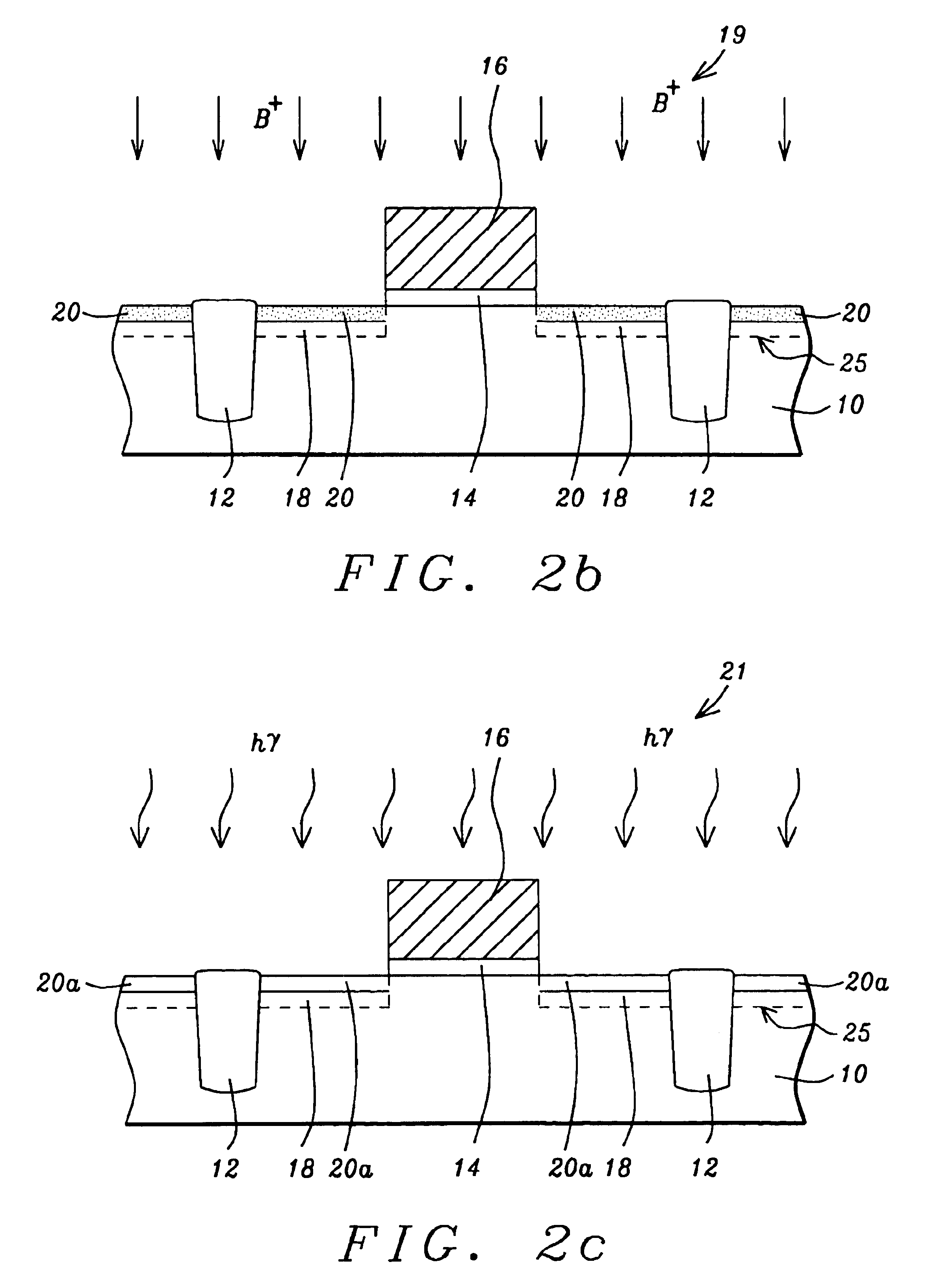
[0023]In a first embodiment of this invention a p-channel self-aligned gate MOSFET is formed with an ultra shallow lightly doped source / drain region on each side of the channel region. Referring to FIG. 2a, an n-type oriented monocrystalline silicon wafer 10 with a resistivity of between about 2 and 50 ohm cm. is provided. Field isolation 12 preferably shallow trench isolation (STI) is formed, defining an enclosed silicon region 8 wherein the device will be formed. The STI regions 12 is formed by the well known method of anisotropically etching a trench surrounding the active silicon device region, growing a between about 100 and 500 Angstrom thick thermal oxide in the trench and then filling the trench by depositing an insulative layer, preferably silicon oxide. The excess silicon oxide above the trench is then removed by CMP (chemical mechanical planarization). Alternately the field isolation 12 may be formed by the familiar LOCOS (local oxidation of silicon) method. A gate oxide...


PUM

PropertyMeasurementUnit
energyaaaaaaaaaa
energyaaaaaaaaaa
thickaaaaaaaaaa

Abstract

A method for forming a highly activated ultra shallow ion implanted semiconductive elements for use in sub-tenth micron MOSFET technology is described. A key feature of the method is the ability to activate the implanted impurity to a highly active state without permitting the dopant to diffuse further to deepen the junction. A selected single crystalline silicon active region is first amorphized by implanting a heavy ion such as silicon or germanium. A semiconductive impurity for example boron is then implanted and activated by pulsed laser annealing whereby the pulse fluence, frequency, and duration are chosen to maintain the amorphized region just below it's melting temperature. It is found that just below the melting temperature there is sufficient local ion mobility to secure the dopant into active positions within the silicon matrix to achieve a high degree of activation with essentially no change in concentration profile. The selection of the proper laser annealing parameters is optimized by observation of the reduction of sheet resistance and concentration profile as measured on a test site. Application of the method is applied to forming a MOS FET and a CMOS device. The additional processing steps required by the invention are applied simultaneously to both n-channel and p-channel devices of the CMOS device pair.

Description

BACKGROUND OF THE INVENTION[0001](1) Field of the Invention[0002]The invention relates to processes for the manufacture of semiconductor devices and more particularly to processes to the formation of MOSFETs (metal oxide silicon field effect transistors).[0003](2) Background of the Invention and Description of Previous Art[0004]Integrated circuits(ICs) are manufactured by first forming discrete semiconductor devices within the surface of silicon wafers. A multi-level metallurgical interconnection network is then formed over the devices contacting their active elements and wiring them together to create the desired circuits. Most of the ICs produced today utilize the MOSFET as the basic semiconductive device. MOSFETs are chosen over their bipolar counterparts because they can be easily manufactured and, because they operate at low voltages and currents, they generate less heat thereby making them well suited for high density circuit designs.[0005]The basic MOSFET (Metal Oxide Semicon...

Claims


Application Information

Patent Timeline
Patent Type & Authority Patents(United States)
IPC IPC(8): H01L21/02H01L21/336H01L21/268H01L21/70H01L21/324H01L21/8238H01L21/265
CPCH01L29/6659H01L21/324H01L21/823814H01L21/268H01L21/26506H01L21/26513H01L21/2658
Inventor POON, CHYIU-HYIACHO, BYUNG JINLU, YONG FENGSEE, ALEXBHAT, MOUSUMI
Owner CHARTERED SEMICONDUCTOR MANUFACTURING
Why Eureka
Try Eureka