High efficiency low cost crystalline-si thin film solar module

a solar module and crystalline-si technology, applied in the field of solar cells, can solve the problems of reducing the efficiency of solar cells, and reducing the absorption of short wavelength ligh

Inactive Publication Date: 2010-12-02
SOLARCITY +1
View PDF11 Cites 95 Cited by
  • Summary
  • Abstract
  • Description
  • Claims
  • Application Information

AI Technical Summary

Benefits of technology

[0015]In a further variation, the MG-Si substrate is removed prior to the formation of the second layer of heavily doped plus intrinsic doped a-Si using one or more of the following techniques: chemical etching, applying a shear or piezoelectric force, applying a temperature gradient, applying an ultra / mega-sonic force, applying a tensile or compressive mechanical force, applying a pressurized water or air jet, shining infrared laser light to cause differential energy absorption, and pumping a pressurized gas into the porous Si layer.

Problems solved by technology

The negative environmental impact caused by the use of fossil fuels and their rising cost have resulted in a dire need for cleaner, cheaper alternative energy sources.
For homojunction solar cells, minority-carrier recombination at the cell surface due to the existence of dangling bonds can significantly reduce the solar cell efficiency; thus, a good surface passivation process is needed.
In addition, the relatively thick, heavily doped emitter layer, which is formed by dopant diffusion, can drastically reduce the absorption of short wavelength light.
Due to the soaring cost of Si material, the existence of such a thick c-Si substrate significantly increases the manufacture cost of existing SHJ solar cells.
However, such an approach has its own limitations in terms of solar cell efficiency.
In addition, the lack of effective passivation between the back surface of the c-Si film and the MG-Si substrate limits the Voc as well as Jsc due to the significant back surface minority carrier recombination.
However, such a process can still consume the c-Si wafer during the transfer.
Moreover, the wafer thickness needs to be more than 500 μm to ensure effective transfer and minimum wafer breakage, making cost an issue.

Method used


Image

  • High efficiency low cost crystalline-si thin film solar module
  • High efficiency low cost crystalline-si thin film solar module
  • High efficiency low cost crystalline-si thin film solar module

Examples


Embodiment Construction

[0038]The following description is presented to enable any person skilled in the art to make and use the embodiments, and is provided in the context of a particular application and its requirements. Various modifications to the disclosed embodiments will be readily apparent to those skilled in the art, and the general principles defined herein may be applied to other embodiments and applications without departing from the spirit and scope of the present disclosure. Thus, the present invention is not limited to the embodiments shown, but is to be accorded the widest scope consistent with the principles and features disclosed herein.

Overview

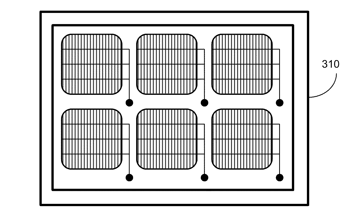
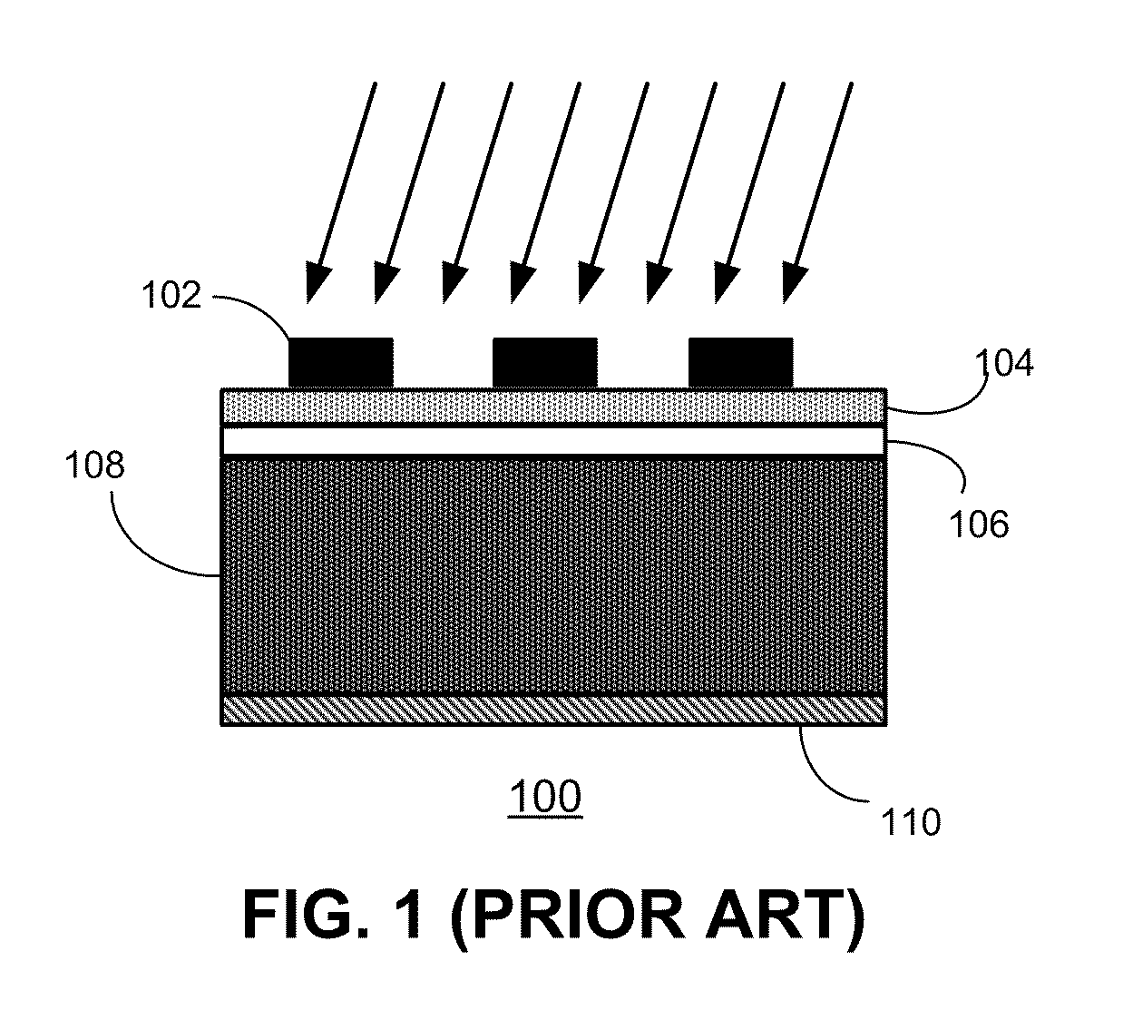
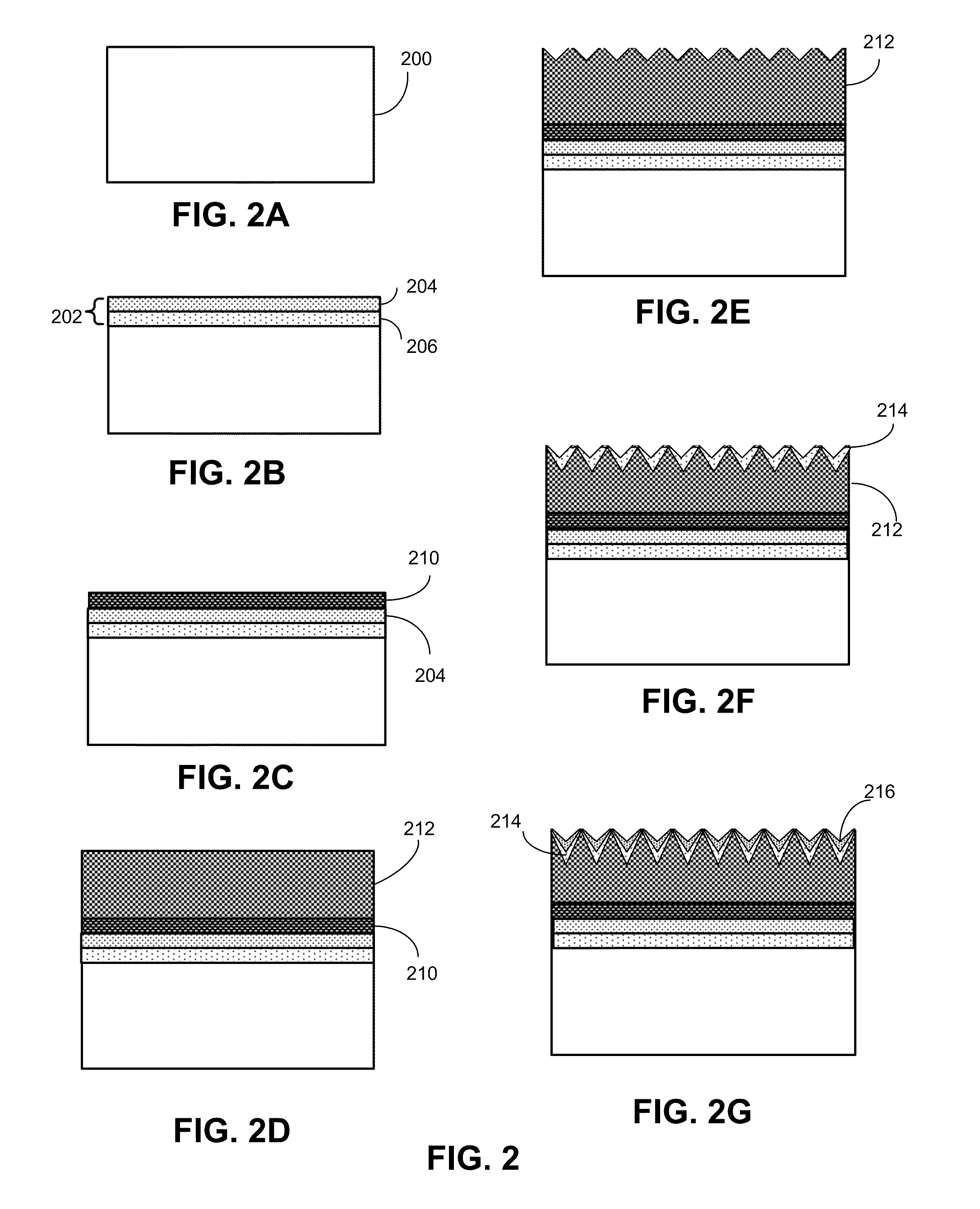
[0039]Embodiments of the present invention provide a “double-sided” heterojunction solar cell module. To fabricate a double-sided heterojunction solar cell, a multilayer heterojunction structure is first deposited on top of an MG-Si substrate. The multilayer structure includes a thin layer of heavily doped c-Si acting as a back-surface-field (BSF) ...


PUM


Abstract

One embodiment of the present invention provides a double-sided heterojunction solar cell module. The solar cell includes a frontside glass cover, a backside cover situated below the frontside glass cover, and a number of solar cells situated between the frontside glass cover and the backside glass cover. Each solar cell includes a semiconductor multilayer structure situated below the frontside glass cover, including: a frontside electrode grid, a first layer of heavily doped amorphous Si (a-Si) situated below the frontside electrode, a layer of lightly doped crystalline-Si (c-Si) situated below the first layer of heavily doped a-Si, and a layer of heavily doped c-Si situated below the lightly doped c-Si layer. The solar cell also includes a second layer of heavily doped a-Si situated below the multilayer structure; and a backside electrode situated below the second layer of heavily doped a-Si.

Description

RELATED APPLICATIONS[0001]This application claims the benefit of U.S. Provisional Application No. 61 / 183,308, Attorney Docket Number SSP09-1007PSP, entitled “High Efficiency, Low Cost Photovoltaic Modules Based on Thin Epitaxial Silicon and Substrate Reuse,” by inventors Jiunn Benjamin Heng, Chentao Yu, Zheng Xu, Jianming Fu, and Peijun Ding, filed 2 Jun. 2009.[0002]This application is a continuation-in-part application of U.S. patent application Ser. No. 12 / 476,991, Attorney Docket Number SSP09-1007, entitled “Low-Cost High-Efficiency Solar Module Using Epitaxial Si Thin-Film Absorber and Double-Sided Heterojunction Solar Cell with Integrated Module Fabrication,” by inventors Jiunn Benjamin Heng, Chentao Yu, Zheng Xu, Jianming Fu, and Peijun Ding, filed 2 Jun. 2009.BACKGROUND[0003]1. Field[0004]This disclosure is generally related to solar cells. More specifically, this disclosure is related to a double-sided heterojunction solar cell and solar cell module fabricated by first epita...

Claims


Application Information

Patent Timeline
Patent Type & Authority Applications(United States)
IPC IPC(8): H01L31/042H01L31/00H01L21/20H01L31/18
CPCH01L31/0236H01L31/028H01L31/0284H01L31/03762Y02E10/547H01L31/1804H01L31/1892B32B17/10036H01L31/048H01L31/02363H01L31/0516H01L31/0684H01L31/0747Y02P70/50
Inventor HENG, JIUNN BENJAMINYU, CHENTAOXU, ZHENGFU, JIANMINGDING, PEIJUN
Owner SOLARCITY
Why Eureka
Try Eureka