

De-fluoridation process
a technology of defluoridation and process, which is applied in the direction of semiconductor/solid-state device manufacturing, basic electric elements, electric apparatus, etc., can solve the problems of unreliable features, additional problems, and short wavelength photoresists used in the use of longer wavelength photoresists
- Summary
- Abstract
- Description
- Claims
- Application Information
AI Technical Summary
Benefits of technology
Problems solved by technology
Method used
Image

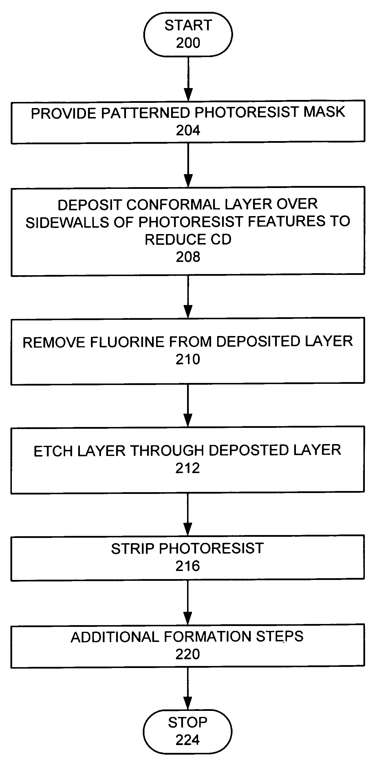
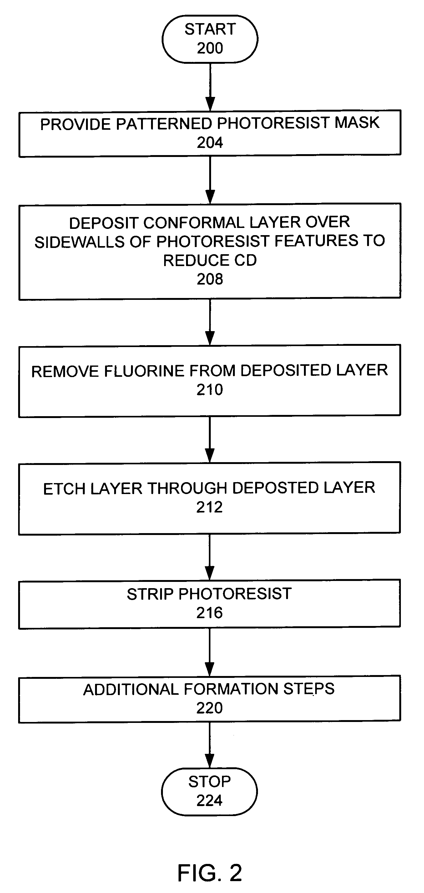
Examples
example recipe
[0077
[0078]In an example recipe, a device that may be used for both depositing and etching the deposition layer and the conductive layer is the 2300 Versys™ made by LAM Research Corporation™ of Fremont, Calif. FIG. 13 is a schematic illustration of such a device 1900 used for both depositing and etching the deposition layer. The plasma processing chamber 1900 comprises an inductive antenna (or coil) 1902, a gas distribution plate (GDP) 1904, a substrate support 1908, a gas source 1910, and an exhaust pump 1920. The gas source 1910 is in fluid connection with the gas distribution plate 1904 and comprises a deposition gas source 1912, a de-fluoridation gas 1914, and an etch gas source 1916. The gas source 1910 may comprise additional gas sources, such as a second etching or deposition gas source. Within plasma processing chamber 1900, the substrate 1604 is positioned upon the substrate support 1908. The substrate support 1908 incorporates a suitable substrate chucking mechanism (e.g.,...
PUM
 Abstract
Description
Claims
Application Information