Waveguide PIN photodiode having graded index distribution centering around optical absorption layer

a waveguide pin and photodiode technology, applied in the field of photodiodes, can solve the problems that the waveguide pin photodiode having a low speed less than 5 ghz is still not available on the market, and achieves the effects of low speed, high responsivity and high coupling coefficien

Inactive Publication Date: 2007-12-18
ELECTRONICS & TELECOMM RES INST
View PDF14 Cites 2 Cited by
  • Summary
  • Abstract
  • Description
  • Claims
  • Application Information

AI Technical Summary

Benefits of technology

[0008]The present invention provides a waveguide PIN photodiode having a low speed less than 5 GHz, high responsivity, a high coupling coefficient when coupled to a single-mode optical fiber, high alignment tolerance, and low package costs.

Problems solved by technology

On the other hand, a waveguide PIN photodiode having a low speed less than 5 GHz is still not available on the market due to high package costs and low demand.

Method used


Image

  • Waveguide PIN photodiode having graded index distribution centering around optical absorption layer
  • Waveguide PIN photodiode having graded index distribution centering around optical absorption layer
  • Waveguide PIN photodiode having graded index distribution centering around optical absorption layer

Examples


Embodiment Construction

[0024]The present invention will now be described more fully with reference to the accompanying drawings, in which exemplary embodiments of the invention are shown. The invention may, however, be embodied in many different forms and should not be construed as being limited to the embodiments set forth herein; rather, these embodiments are provided so that this disclosure will be thorough and complete, and will fully convey the concept of the invention to those skilled in the art. In the drawings, the thicknesses of layers and regions are exaggerated for clarity.

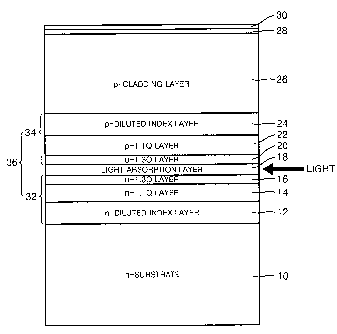
[0025]FIG. 1 is a sectional view of a waveguide PIN photodiode according to an embodiment of the present invention.

[0026]In detail, FIG. 1 illustrates a cross-section of a crystal growth of the waveguide PIN photodiode of FIG. 1. The waveguide PIN photodiode includes a light absorption layer 18 formed on a substrate 10, for example, in a central portion on an InP substrate. The light absorption layer 18 may be formed of InGaA...


PUM


Abstract

A waveguide PIN photodiode is provided. The waveguide PIN photodiode includes a lower light guide layer, a light absorption layer, an upper light guide layer, and a cladding layer. The lower light guide is formed on a substrate, and the light absorption layer is formed on the lower light guide layer. The upper light guide layer is formed on the light absorption layer, and the cladding layer is formed on the upper light guide layer. The lower light guide layer, the light absorption layer, and the upper light guide layer constitute a core layer, which is an optical waveguide, and graded index distribution is symmetrically formed in a depth direction, centering around the light absorption layer having a highest refractive index.

Description

CROSS-REFERENCE TO RELATED PATENT APPLICATION[0001]This application claims the benefit of Korean Patent Application No. 10-2005-0121242, filed on Dec. 10, 2005, in the Korean Intellectual Property Office, the disclosure of which is incorporated herein in its entirety by reference.BACKGROUND OF THE INVENTION[0002]1. Field of the Invention[0003]The present invention relates to a photodiode, and more particularly, to a waveguide PIN (p-type, intrinsic, n-type) photodiode.[0004]2. Description of the Related Art[0005]Photodiodes are essential parts in local area optical networks such as wavelength division multiplexing (WDM)-passive optical networks (PONs) and e-PONs. Research on optical communication technologies is being actively pursued and ultra-high technology optical communication is widely used for a long distance back-bone network. However, coaxial cables are used as the main communication means for local area access networks, i.e., data communication between a base station and a...

Claims


Application Information

Patent Timeline
Patent Type & Authority Patents(United States)
IPC IPC(8): G02B6/10G02B6/26H04B10/06
CPCG02B6/12004H01L31/105H01L31/0304H01L31/10
Inventor PARK, SAHNG GISIM, EUN DEOKPARK, JEONG WOOSIM, JAE SIKBAEK, YONG SOON
Owner ELECTRONICS & TELECOMM RES INST
Why Eureka
Try Eureka