Switching power supply device

a power supply device and switching technology, applied in the direction of electric variable regulation, process and machine control, instruments, etc., can solve the problems of circuit damage, long time for reverse recovery, and general lowering of output voltag

Inactive Publication Date: 2008-01-01
SANKEN ELECTRIC CO LTD
View PDF7 Cites 55 Cited by
  • Summary
  • Abstract
  • Description
  • Claims
  • Application Information

AI Technical Summary

Benefits of technology

[0027]It is an object of the present invention to provide a switching power supply device in which a first switching element and a second switching element can be prevented from being in a state of a short-circuit even when they fall into a state of resonance deviation at the time of overloading or starting-up.
[0030]That is, even in a state where the cyclic current becomes negative when the one switching element is off, an output voltage decreases to reset the exciting energy, and the other switching element is not turned on until the current of the one switching element is turned off. Therefore, a through-current caused by a reverse recovery time of the body diode of the one switching element can be prevented when the other switching element is turned on.
[0031]In a second aspect of the present invention, there are provided a series circuit in which a first switching element and a second switching element are connected in series at both ends of an output of an input rectifier circuit for rectifying alternating voltage of an alternating current power supply or at both ends of a direct current power supply, a resonant circuit in which a primary winding of a transformer and a current resonant capacitor are connected in series at both ends of the first switching element or the second switching element, at least one pair of rectifying and smoothing circuit for rectifying and smoothing a voltage generated across a secondary winding of the transformer during an on-period of any one of the first switching element and the second switching element, a control circuit for alternately turning on / off the first switching element and the second switching element based on a voltage from the at least one pair of the rectifying and smoothing circuits, and a voltage detecting circuit for outputting a voltage detecting signal when the voltage at both ends of one switching element of the first switching element and the second switching element, which are turned off at a time of transmitting electric power to the at least one pair of the rectifying and smoothing circuits, becomes equal to a predetermined voltage or less. The control circuit turns on the one switching element based on the voltage detecting signal from the voltage detecting circuit. According to the second aspect of the present invention, effects similar to the effects of the first aspect of the present invention can be obtained.
[0035]In a sixth aspect of the present invention, in place of the voltage detecting circuit, an output voltage detecting circuit for detecting an output voltage is provided. The control circuit turns on the other switching element of the first switching element and the second switching element after a predetermined period has passed since the one switching element is turned off in the case where the output voltage from the output voltage detecting circuit is equal to a predetermined voltage or less when the one switching element of the first switching element and the second switching element, which is turned on at the time of transmitting electric power to the at least one pair of the rectifying and smoothing circuits, is turned off, and changes the predetermined period according to the output voltage. Therefore, the other switching element can be turned on after the exciting energy of the transformer is sufficiently reset. With this, the cyclic current caused by the reverse recovery time of the body diode of the one switching element can be prevented when the other switching element is turned on.

Problems solved by technology

In addition, when the output current becomes overloaded, the output voltage is generally lowered because electric power is limited due to over-current protection.
In general, a body diode which is parasitically formed in a switching element takes a long time for reverse recovery, and thus large current flows therein.
In the worst case, the circuit may be damaged.
Therefore, it is difficult that the switching element Q1 is turned on after the switching element Q2 is turned off during this rapid current change.
2005-51918, a loss is caused in the current state detecting circuit and efficiency is deteriorated.

Method used


Image

  • Switching power supply device
  • Switching power supply device
  • Switching power supply device

Examples


first embodiment

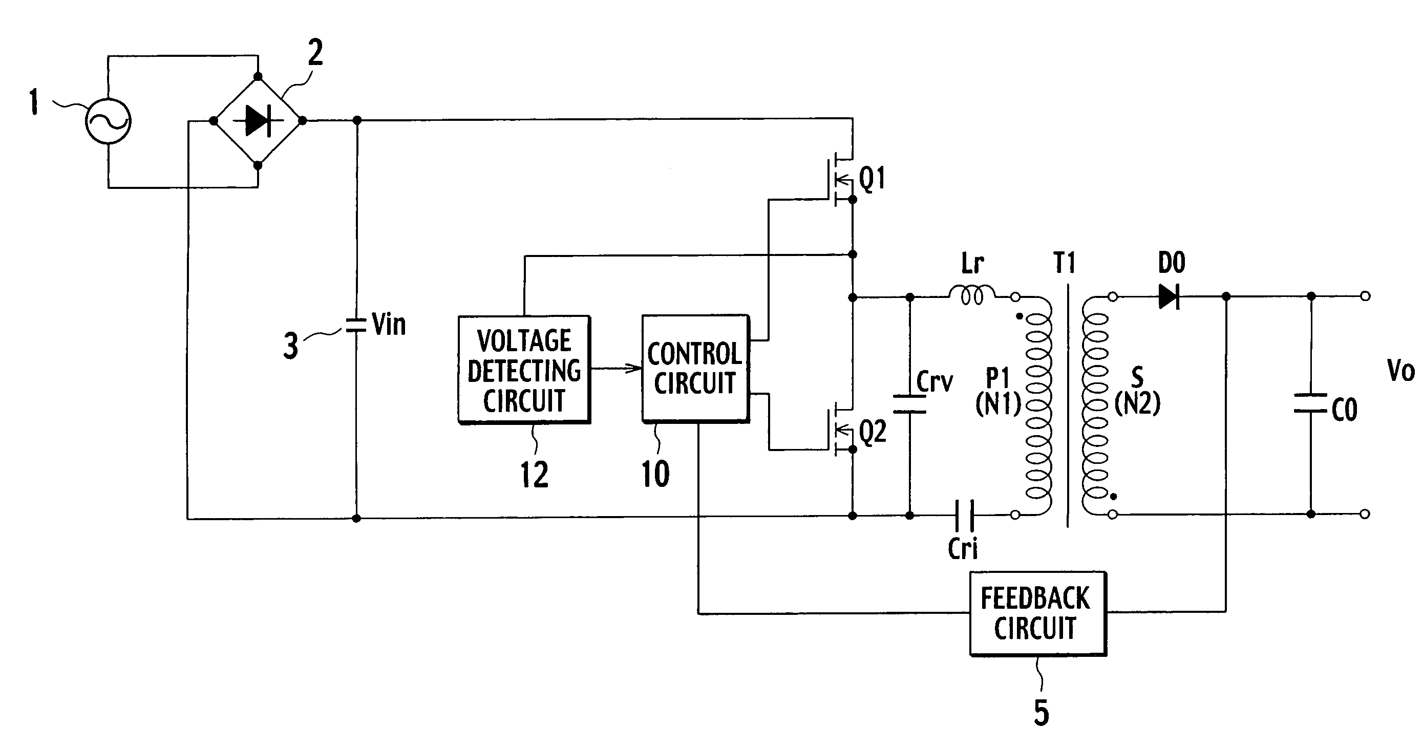
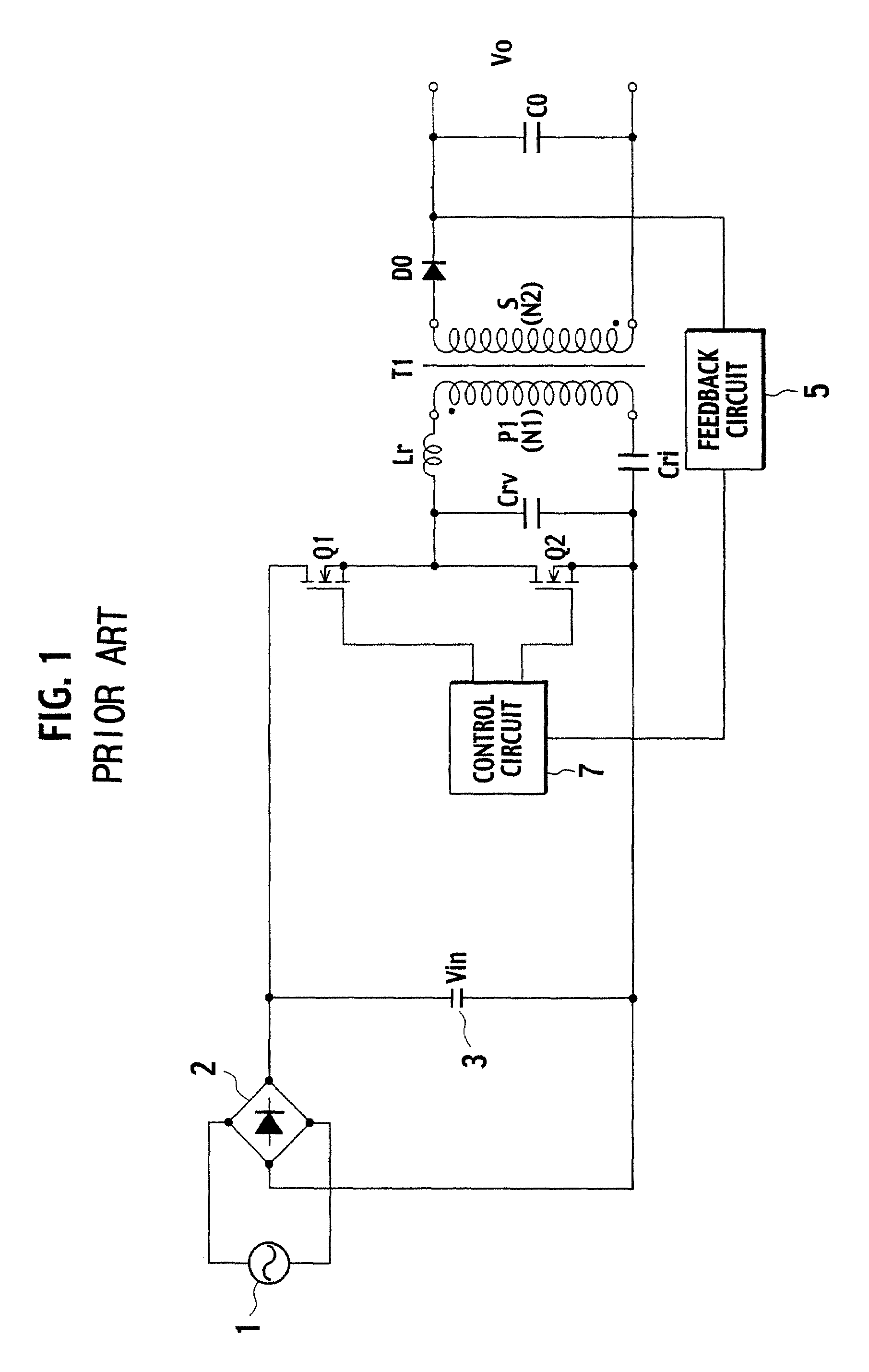
[0055]FIG. 5 is a circuit configuration diagram for showing a switching power supply device according to a first embodiment of the present invention. In relation to the conventional switching power supply device shown in FIG. 1, the switching power supply device of the first embodiment shown in FIG. 5 is characterized by including a voltage detecting circuit 12 connected to a connecting point of a switching element Q1 and a switching element Q2, and a control circuit 10.

[0056]In FIG. 5, a full-wave rectifier circuit 2 (which corresponds to an input rectifier circuit) rectifies alternating voltage of an alternating current power supply 1 for commercial use to output full-wave rectifying voltage to a smoothing capacitor 3. The smoothing capacitor 3 obtains a direct current power supply Vin by smoothing the full-wave rectifying voltage of the full-wave rectifier circuit 2.

[0057]At both ends of this smoothing capacitor 3, a series circuit of the switching element Q1 consisting of MOSFET...

second embodiment

[0089]A switching power supply device according to a second embodiment monitors a voltage at both ends of a switching element Q2 just after the switching element Q2 is turned off, and prevents a switching element Q1 from being turned on for a predetermined period in order to sufficiently reset a exciting current of an exciting inductance of a primary winding P1 when the voltage does not increase just after the switching element Q2 is turned off, that is in the case where a cyclic current flows through a body diode when the switching element Q2 is off.

[0090]The second embodiment has a substantially similar circuit configuration with the circuit configuration of the first embodiment shown in FIG. 5, and is different in configurations of a voltage detecting circuit 12c and a control circuit 10a shown in FIG. 9. Here, only different parts in the configuration shown in FIG. 9 in relation to the configuration shown in FIG. 6 will be described.

[0091]In the voltage detecting circuit 12c sho...

third embodiment

[0108]FIG. 11 is a circuit configuration diagram for showing details of a voltage detecting circuit and a control circuit of a switching power supply according to a third embodiment.

[0109]In relation to the circuit configuration of the second embodiment shown in FIG. 9, the third embodiment is different in that the voltage detecting circuit 12c is removed, an auxiliary winding P2 is provided, and a configuration of a control circuit 10b shown in FIG. 11 is different. Here, only different parts in the configuration shown in FIG. 11 in relation to the configuration shown in FIG. 9 will be described.

[0110]The control circuit 10b turns on a switching element Q1 after a predetermined period has passed since a switching element Q2 is turned off in the case where a voltage at both ends of the switching element Q2 does not reach at a predetermined voltage when the switching element Q2 is turned off, and changes the predetermined time according to an output voltage from the auxiliary winding...


PUM


Abstract

A series circuit in which a first switching element and a second switching element are connected in series at both ends of an output of an input rectifier circuit for rectifying an alternating current of an alternating current power supply, a resonant circuit in which a primary winding of a transformer and a current resonant capacitor are connected in series at both ends of the first switching element or the second switching element, a rectifying and smoothing circuit for rectifying and smoothing a voltage generated across a secondary winding of the transformer during an on-period of the first switching element or the second switching element, a control circuit for alternately turning on / off the first switching element and the second switching based on a voltage from the rectifying and smoothing circuit, and a voltage detecting circuit for outputting a voltage detecting signal when a voltage at both ends of one switching element of the first switching element and the second switching element, which is turned on at a time of transmitting electric power to the rectifying and smoothing circuit, becomes equal to a predetermined voltage or more. The control circuit turns on the other switching element of the first switching element and the second switching element based on the voltage detecting signal from the voltage detecting circuit.

Description

BACKGROUND OF THE INVENTION[0001]1. Field of the Invention[0002]The present invention relates to a resonant-type switching power supply device. Specifically, the present invention relates to prevention of a through-current in a switching power supply device.[0003]2. Description of the Related Art[0004]FIG. 1 is a circuit configuration diagram of a conventional resonant-type switching power supply device. In FIG. 1, a full-wave rectifier circuit 2 (which corresponds to an input rectifier circuit) rectifies an alternating current of an alternating current power supply 1 for commercial use to output a full-wave rectifying voltage to a smoothing capacitor 3. The smoothing capacitor 3 obtains a direct current power supply Vin by smoothing the full-wave rectifying voltage of the full-wave rectifier circuit 2.[0005]At both ends of the smoothing capacitor 3, a series circuit including a switching element Q1 consisting of a MOSFET or the like and a switching element Q2 consisting of a MOSFET...

Claims


Application Information

Patent Timeline
Patent Type & Authority Patents(United States)
IPC IPC(8): H02M3/335
CPCH02M3/337Y02B70/1433H02M1/38Y02B70/10H02M1/0058H02M3/33571H02M3/01H02M3/28
Inventor KYONO, YOICHI
Owner SANKEN ELECTRIC CO LTD
Why Eureka
Try Eureka