Substrate contact for a capped MEMS and method of making the substrate contact at the wafer level

a technology of substrate contact and capped mems, which is applied in the field of microelectromechanical systems, can solve the problems of increasing the size of the mems accelerometer, experiencing parasitic capacitance from the device during operation, and difficulty in handling and bonding the bond wir

Inactive Publication Date: 2008-01-08
NORTH STAR INNOVATIONS
View PDF4 Cites 16 Cited by
  • Summary
  • Abstract
  • Description
  • Claims
  • Application Information

AI Technical Summary

Benefits of technology

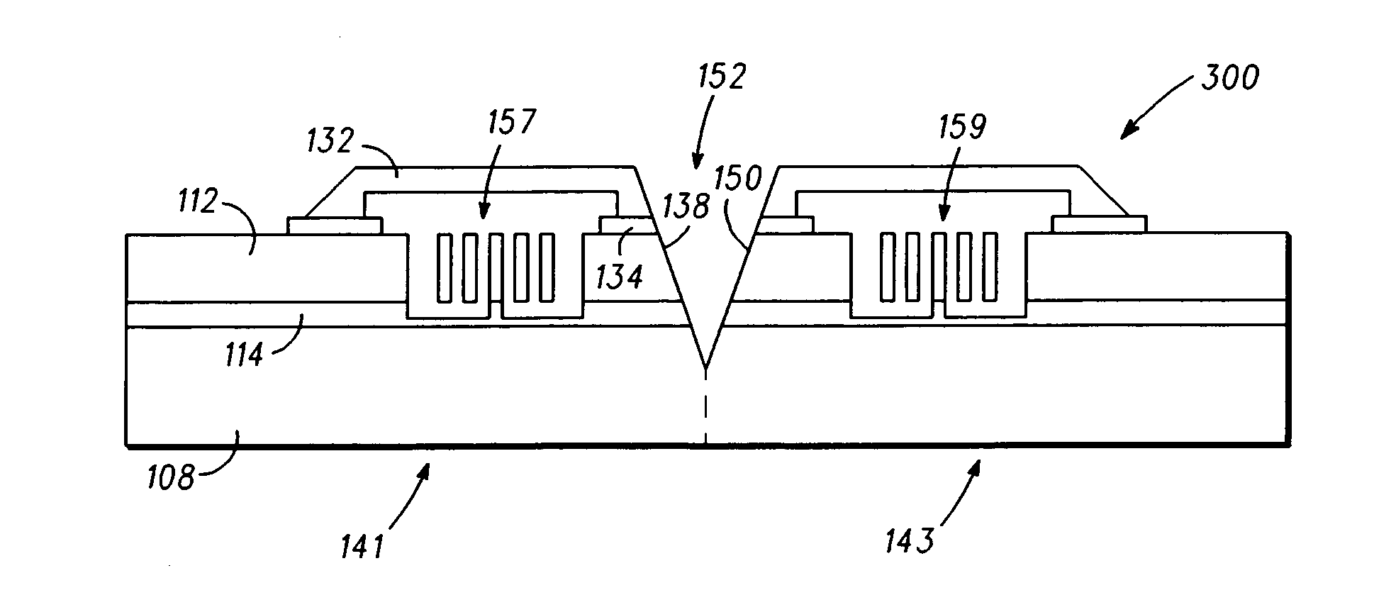
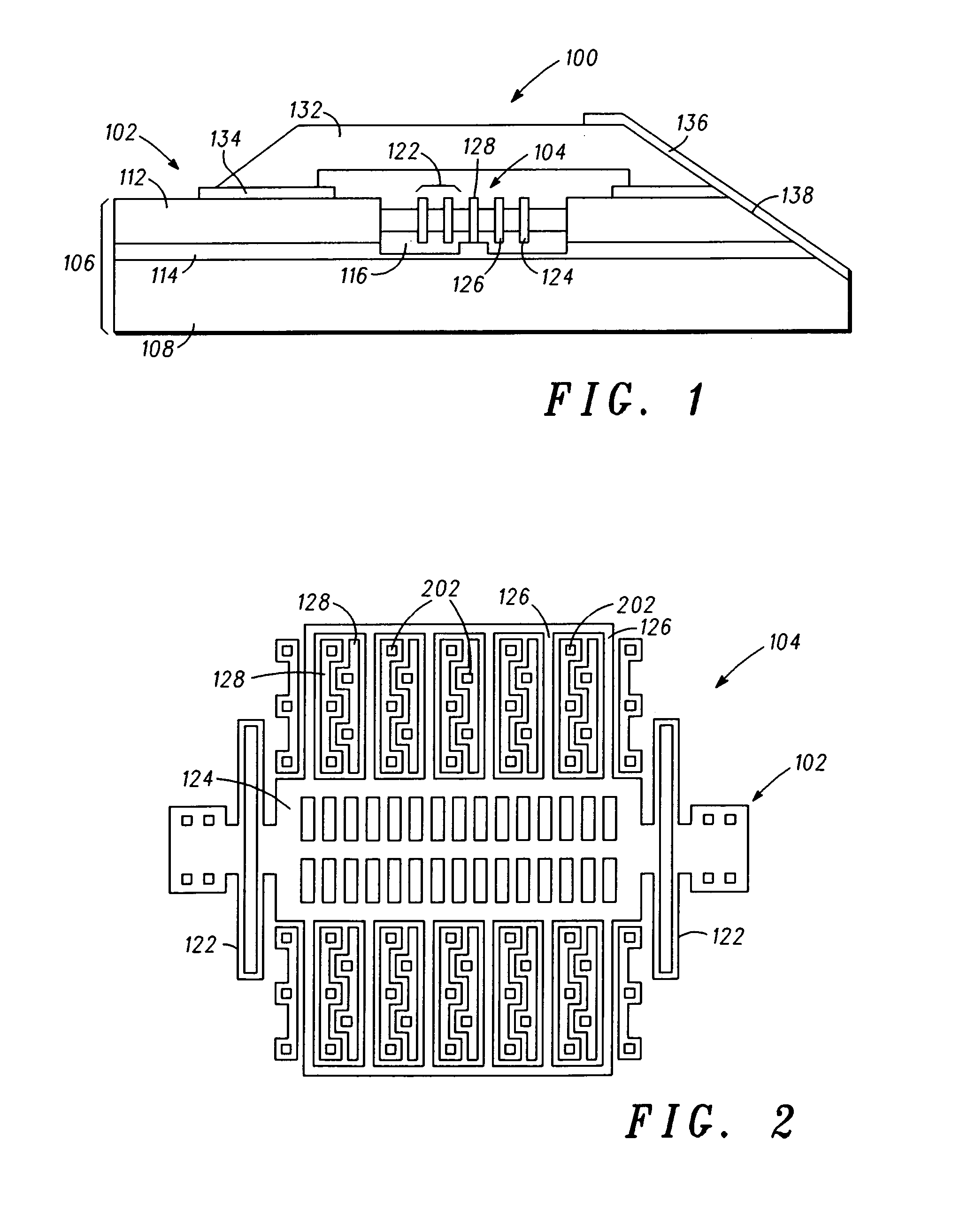
[0020]Interconnect 136 grounds protective cap 132 to handle layer 108 to prevent parasitic capacitance from interfering with the above-mentioned capacitance measurement. Preferably, interconnect 136 is coupled to a sidewall 138 that is defined by edges of active layer 112, sacrificial layer 114, protective cap 132, and cap anchor 134. Interconnect 136 is adhered to sidewall 138 such that at least protective cap 132 and handle layer 108 are electrically coupled. Alternatively, interconnect 136 may extend beyond sidewall 138 and may cover other portions of protective cap 132, such as a top portion.

Problems solved by technology

Each device may emit electromagnetic interference waves, and, if the MEMS accelerometer is placed too close to another device, it may experience parasitic capacitance from the device during operation.
MEMS accelerometers are increasingly becoming smaller, thus, bond wires having fine and ultra-fine pitches and decreased diameters are typically used; however, these bond wires may have certain drawbacks.
For example, the decreased pitch and diameter may cause difficulties in handling and bonding the bond wires.
In particular, the bond wires may unintentionally short to other conductive structures of the MEMS accelerometer.
Additionally, attaching bond wires to the components is a relatively expensive process.

Method used


Image

  • Substrate contact for a capped MEMS and method of making the substrate contact at the wafer level
  • Substrate contact for a capped MEMS and method of making the substrate contact at the wafer level
  • Substrate contact for a capped MEMS and method of making the substrate contact at the wafer level

Examples


Embodiment Construction

[0014]The following detailed description is merely exemplary in nature and is not intended to limit the invention or the application and uses of the invention. Furthermore, there is no intention to be bound by any expressed or implied theory presented in the preceding technical field, background, brief summary or the following detailed description. In this regard, although the invention is depicted and described in the context of an accelerometer, it will be appreciated that the invention at least could be used for any one of numerous devices that include a proof mass movably suspended above a substrate surface or any microelectromechanical systems (“MEMS”) device that may need protection from electromagnetic interference.

[0015]Turning now to the description, FIG. 1 is a cross-sectional view of an exemplary MEMS device 100. MEMS device 100 is an inertial sensor, such as an accelerometer, and includes a field region 102 and a sensor region 104 formed on a wafer 106. Wafer 106 may be ...


PUM


Abstract

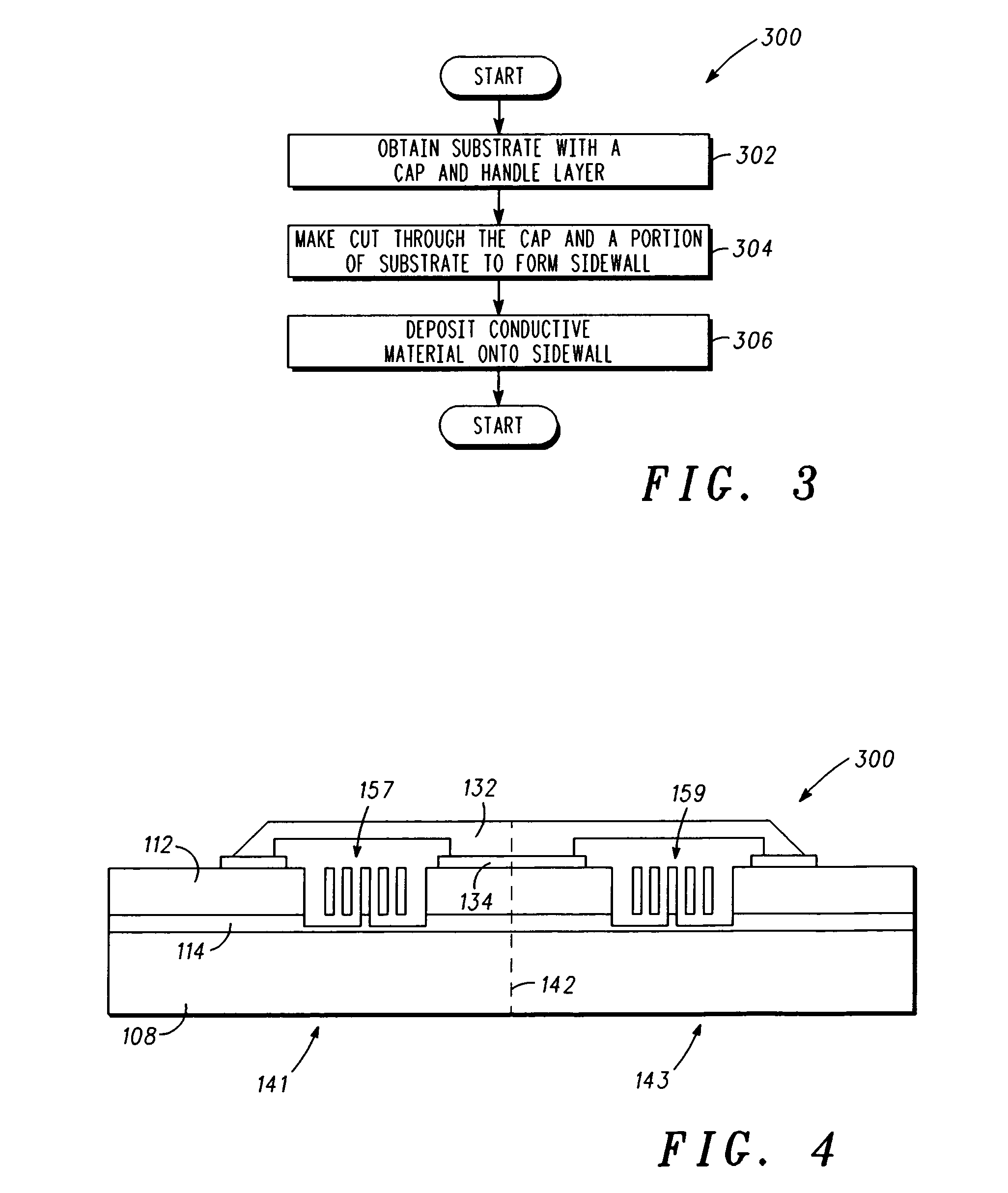
A MEMS device (100) is provided that includes a handle layer (108) having a sidewall (138), a cap (132) overlying said handle layer (108), said cap (132) having a sidewall (138), and a conductive material (136) disposed on at least a portion of said sidewall of said cap (138) and said sidewall of said handle layer (138) to thereby electrically couple said handle layer (108) to said cap (132). A wafer-level method for manufacturing the MEMS device from a substrate (300) comprising a handle layer (108) and a cap (132) overlying the handle layer (108) is also provided. The method includes making a first cut through the cap (132) and at least a portion of the substrate (300) to form a first sidewall (138), and depositing a conductive material (136) onto the first sidewall (138) to electrically couple the cap (132) to the substrate (300).

Description

FIELD OF THE INVENTION[0001]The present invention generally relates to micro-electromechanical systems (“MEMS”), and more particularly relates to establishing contacts for use on MEMS.BACKGROUND OF THE INVENTION[0002]Many devices and systems include a number of different types of sensors that perform various monitoring and / or control functions. Advancements in micromachining and other microfabrication processes have enabled the manufacturing of a wide variety of microelectromechanical systems (“MEMS”) devices. In recent years, many of the sensors that are used to perform monitoring and / or control functions have been implemented into MEMS devices.[0003]One particular type of MEMS sensor is an accelerometer. Typically, a MEMS accelerometer includes, among other component parts, a proof mass that may be constructed on a silicon-on-insulator wafer. The proof mass is resiliently suspended by one or more suspension springs to one section of the wafer. The proof mass moves when the MEMS ac...

Claims


Application Information

Patent Timeline
Patent Type & Authority Patents(United States)
IPC IPC(8): H01L21/00B81C99/00
CPCG01P15/0802G01P15/125B81B3/0086G01P2015/0814B81B2201/0235B81B2207/07B81B2207/098B81C2203/0118
Inventor HOOPER, STEPHEN R.DESAI, HEMANT D.MCDONALD, WILLIAM G.SALIAN, ARVIND S.
Owner NORTH STAR INNOVATIONS
Why Eureka
Try Eureka