Nonvolatile semiconductor memory, a data write-in method for the nonvolatile semiconductor memory and a memory card

a nonvolatile semiconductor and data write-in technology, applied in static storage, digital storage, instruments, etc., can solve the problems of program disturbance, program disturbance, and program disturbance in all pages

Active Publication Date: 2008-01-08
KIOXIA CORP
View PDF8 Cites 44 Cited by
  • Summary
  • Abstract
  • Description
  • Claims
  • Application Information

AI Technical Summary

Problems solved by technology

A problem arises that a program disturbance frequently occurs due to an unselected voltage.
In addition, since a write-in loop runs until data is written in all memory cell transistors, or until the Loop—max in a page, which includes several bits of low write-in speed memory cell transistors, a program disturbance frequently occurs due to an unselected voltage.
Furthermore, there is a problem that a program disturbance frequently occurs in all pages of a nonvolatile semiconductor memory including a ‘column failure’ where ‘0’ is changed to ‘1’ along the bit line length.
In addition, even with a conventional NAND flash memory, setting an upper limit value for a write-in voltage and limiting the write-in voltage below that upper limit value suppresses the influence of a program disturbance, however, there is a problem that write-in yield is adversely affected.

Method used


Image

  • Nonvolatile semiconductor memory, a data write-in method for the nonvolatile semiconductor memory and a memory card
  • Nonvolatile semiconductor memory, a data write-in method for the nonvolatile semiconductor memory and a memory card
  • Nonvolatile semiconductor memory, a data write-in method for the nonvolatile semiconductor memory and a memory card

Examples


first embodiment

[0035]In the following description, a primary specific number of bits is referred to as M1 bits, and a secondary specific number of bits is referred to as M2 bits. In general, there is a principal constraint of M12121 and M2 are arbitrary values, respectively. The larger the value, the more effectively the suppression of influence of a program disturbance. However, the value needs to be equal to or less than the number of fail bits to be ensured of correction when using ECC.

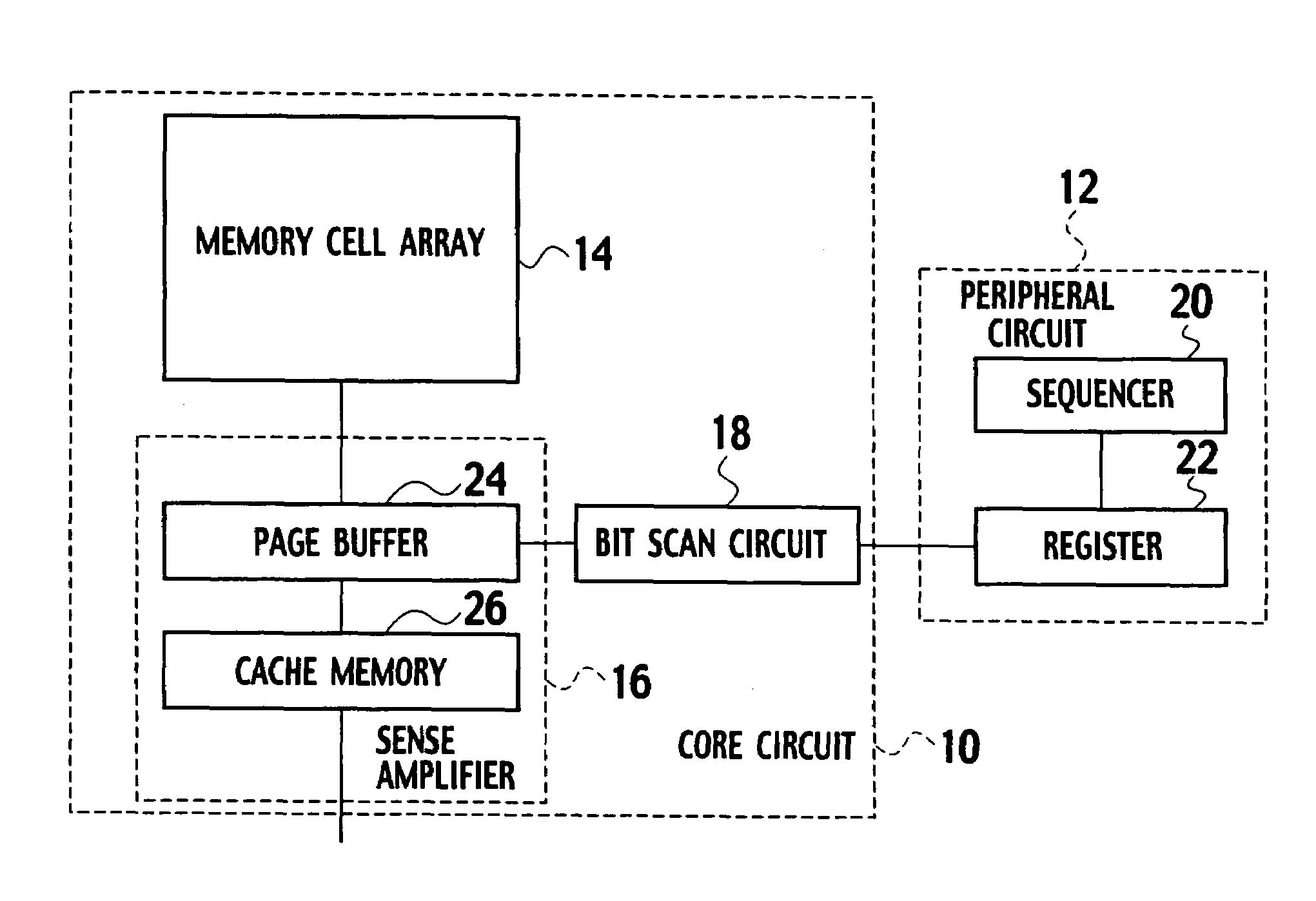
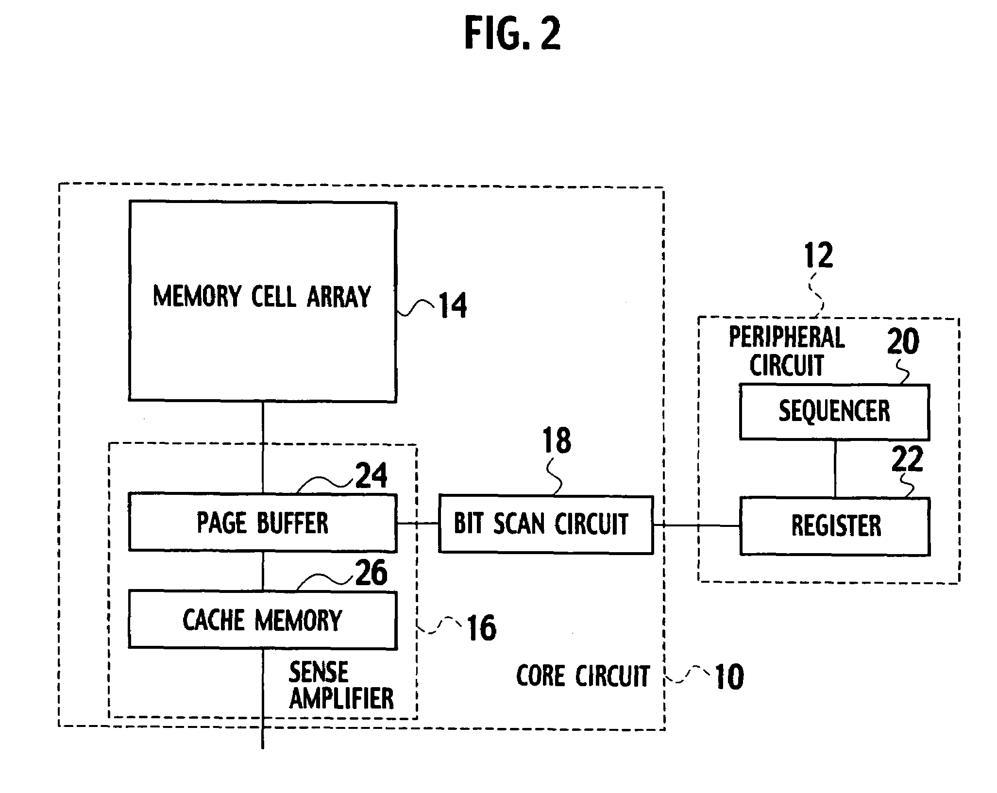
[0036]According to the embodiments of the present invention, a sequencer performs an important operation, such as carrying out bit scan during a write-in operation and terminating the write-in operation if the number of fail bits falls below a specific value. Such operation may be carried out independent of binary or multi-valued logic. In the case of a multi-valued logic, since distance between the threshold voltages is narrow, the multi-valued logic is easily influenced by a program disturbance in a write-in op...

study example

(Study Example)

[0049]A flowchart of FIG. 5 shows a data write-in method for a nonvolatile semiconductor memory, according to a study example for the embodiments of the present invention. Vpgm denotes a write-in voltage, and PC denotes a write-in loop execution count.

[0050]In step S1, the write-in voltage Vpgm is specified to be equal to a start voltage Vpgm—start, and the write-in loop execution count PC is initialized to 0.

[0051]Next, in step S2, the PC is incremented by one.

[0052]Next, in step S3, it is determined whether or not verification status result is pass.

[0053]If Yes in step S3, the process proceeds to step S5, and the status result is pass.

[0054]If No in step S3, the process proceeds to step S4 in which it is then determined whether or not the write-in loop execution count PC is less than the maximum value PC—max of the write-in loop execution count.

[0055]If No in step S4, the process proceeds to step S6, and the status result is fail.

[0056]If Yes in step S4, the process...

second embodiment

[0098]FIG. 13 is a flowchart describing a data write-in method for a nonvolatile semiconductor memory, according to the second embodiment of the present invention.

[0099]According to the first embodiment, bit ignoring parameters are specified based on the data write-in loop execution count. On the other hand, according to the second embodiment, Vpgmx=Vpgm—start+Vx (pgm—max) is given for the write-in start voltage (referred to as Vpgm—start). The loop runs ignoring M1 bit from the start of write-in operation until Vpgmx, and afterwards ignoring M2 bit until Vpgmmax. Bit ignoring parameters are specified in voltages such that the same advantages as those in the first embodiment are achieved.

[0100]According to the nonvolatile semiconductor memory of the second embodiment of the present invention, Loop—max2 is specified to be equal to a specified value Vpgmx which is the sum of the write-in start voltage Vpgm—start and an arbitrary fixed voltage Vx as a variable, and differs for respecti...


PUM


Abstract

A nonvolatile semiconductor memory includes a memory cell array, a page buffer that is connected to the memory cell array and retains program verification results of a write-in operation of repeating data write-in and program verification, a bit scan circuit that is connected to the page buffer and determines whether or not the number of fail bits is equal to or less than number of reference bits based on the program verification results retained in the page buffer, a register that is connected to the bit scan circuit and retains determination results of the bit scan circuit, and a sequencer that controls the write-in operation and an operating sequence of the bit scan circuit and terminates the write-in operation while leaving the number of fail bits in response to the results temporarily stored in the register.

Description

CROSS REFERENCE TO RELATED APPLICATIONS AND INCORPORATION BY REFERENCE[0001]This application is based upon and claims the benefit of priority from prior Japanese Patent Application P2004-175884 filed on Jun. 14, 2004; the entire contents of which are incorporated by reference herein.BACKGROUND OF THE INVENTION[0002]1. Field of the Invention[0003]The present invention relates to a nonvolatile semiconductor memory. More specifically, it relates to a nonvolatile semiconductor memory, a data write-in method for the nonvolatile semiconductor memory and a memory card implementing the nonvolatile semiconductor memory, which suppress program disturbances arising due to an unselected high voltage being applied during a data write-in operation.[0004]2. Description of the Related Art[0005]According to a conventional data write-in method for a NAND flash memory, a program loop for writing data is repeated with an arbitrary step width and is stopped when all bits are written. The arbitrary step ...

Claims


Application Information

Patent Timeline
Patent Type & Authority Patents(United States)
IPC IPC(8): G11C16/06G11C16/02G11C11/34G11C11/56G11C16/34
CPCG11C11/5628G11C16/0483G11C16/3418G11C16/3427G11C16/3454G11C16/3459G11C2211/5621G11C2211/5642G11C16/34G11C16/04G11C16/02G11C29/00
Inventor IDE, YUGOKANEBAKO, KAZUNORI
Owner KIOXIA CORP
Why Eureka
Try Eureka