Semiconductor integrated circuit

a technology of integrated circuits and semiconductors, applied in the direction of generating/distributing signals, pulse techniques, instruments, etc., can solve the problems of increasing chip cost, large circuit area, and increasing testing costs

Inactive Publication Date: 2008-01-15
SOCIONEXT INC
View PDF13 Cites 13 Cited by
  • Summary
  • Abstract
  • Description
  • Claims
  • Application Information

AI Technical Summary

Benefits of technology

[0008]It is an object of the present invention to provide a circuitry technology in which it is able to evaluate the operation margin a semiconductor integrated circuit even if it is supplied from an LSI tester with clocks with a frequency lower than one necessary for the evaluation. In other words, the object is to test a semiconductor integrated circuit at lower cost by using an LSI tester of a low clock frequency.
[0009]According to one of the aspects of the present invention, external clock terminals receive a plurality of external clocks having phases shifted in sequence, respectively. A phase adjustment unit adjusts the phases of the external clocks to generate a plurality of internal clocks with a same phase difference between every adjacent transition edges thereof. A clock composite unit synthesizes the internal clocks to generate a composite clock having a frequency higher than that of the external clocks. An internal circuit operates in synchronization with the composite clock. The phase adjustment unit equalizes all the phase differences between the adjacent internal clocks. All pulse intervals of the composite clock can thus be made equal. Consequently, even when the semiconductor integrated circuit is supplied with external clocks of lower frequencies, it is possible to operate the semiconductor integrated circuit at high speed. For example, the internal circuit can be operated at high speed for testing by using a low-cost LSI tester having a low clock frequency. As a result, it is possible to reduce the testing cost of the semiconductor integrated circuit, allowing a reduction in chip cost.

Problems solved by technology

Testing a semiconductor integrated circuit with clocks of higher frequencies, however, requires expensive LSI testers, which can increase the testing cost.
Nevertheless, PLL circuits contain analog circuits and thus are large in circuit area.
Consequently, the semiconductor integrated circuit may increase in chip area, with an increase in chip cost.
This technique, however, can only generate a clock having a frequency twice that of the external clock.

Method used


Image

  • Semiconductor integrated circuit
  • Semiconductor integrated circuit
  • Semiconductor integrated circuit

Examples


Embodiment Construction

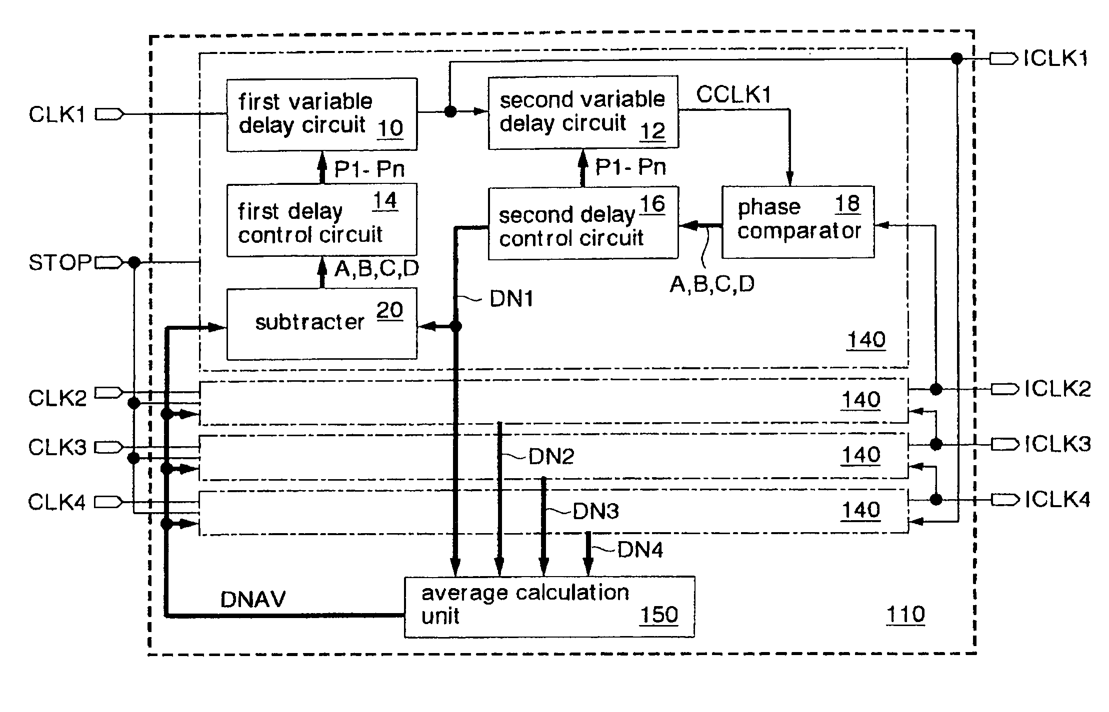
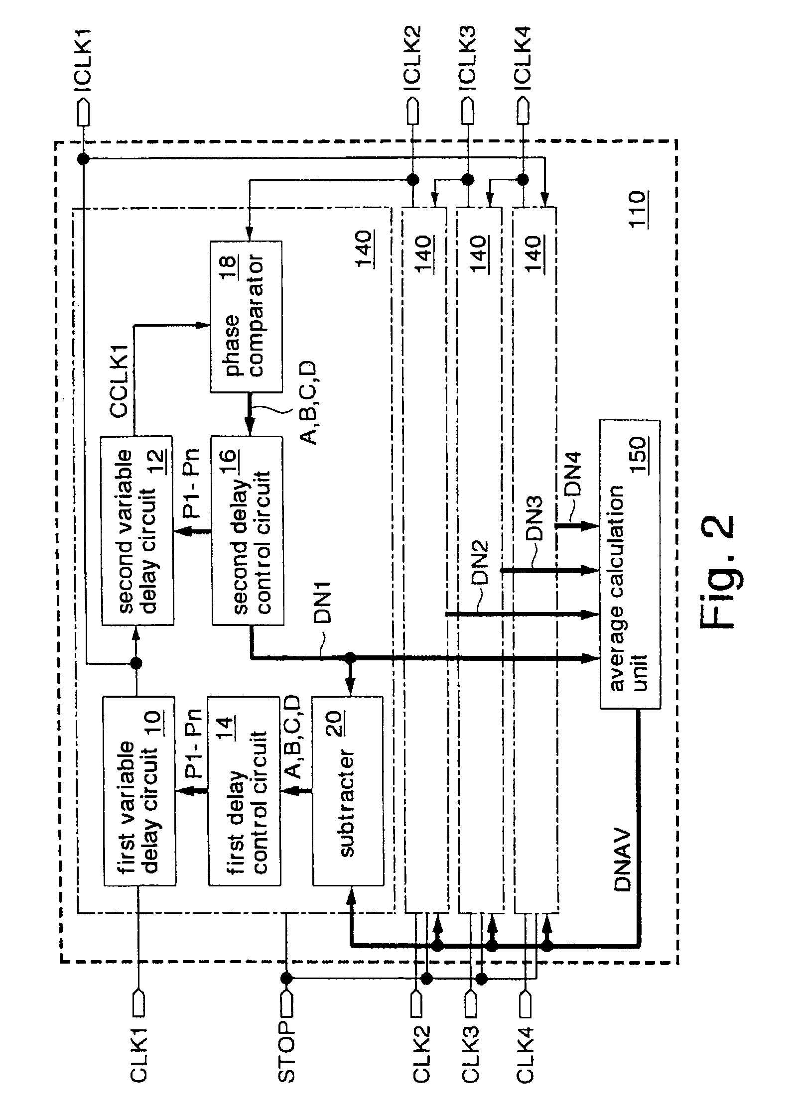
[0053]Embodiments of the present invention will be described with reference to the drawings. Double circles in the drawings represent external terminals. In the drawings, each thick line represents a signal line that consists of a plurality of lines. Some of the blocks connected with the thick lines consist of a plurality of circuits each. Signals supplied through the external terminals are designated by reference symbols identical to the names of the terminals. Signal lines for transmitting signals are designated by reference symbols identical to the names of the signals.

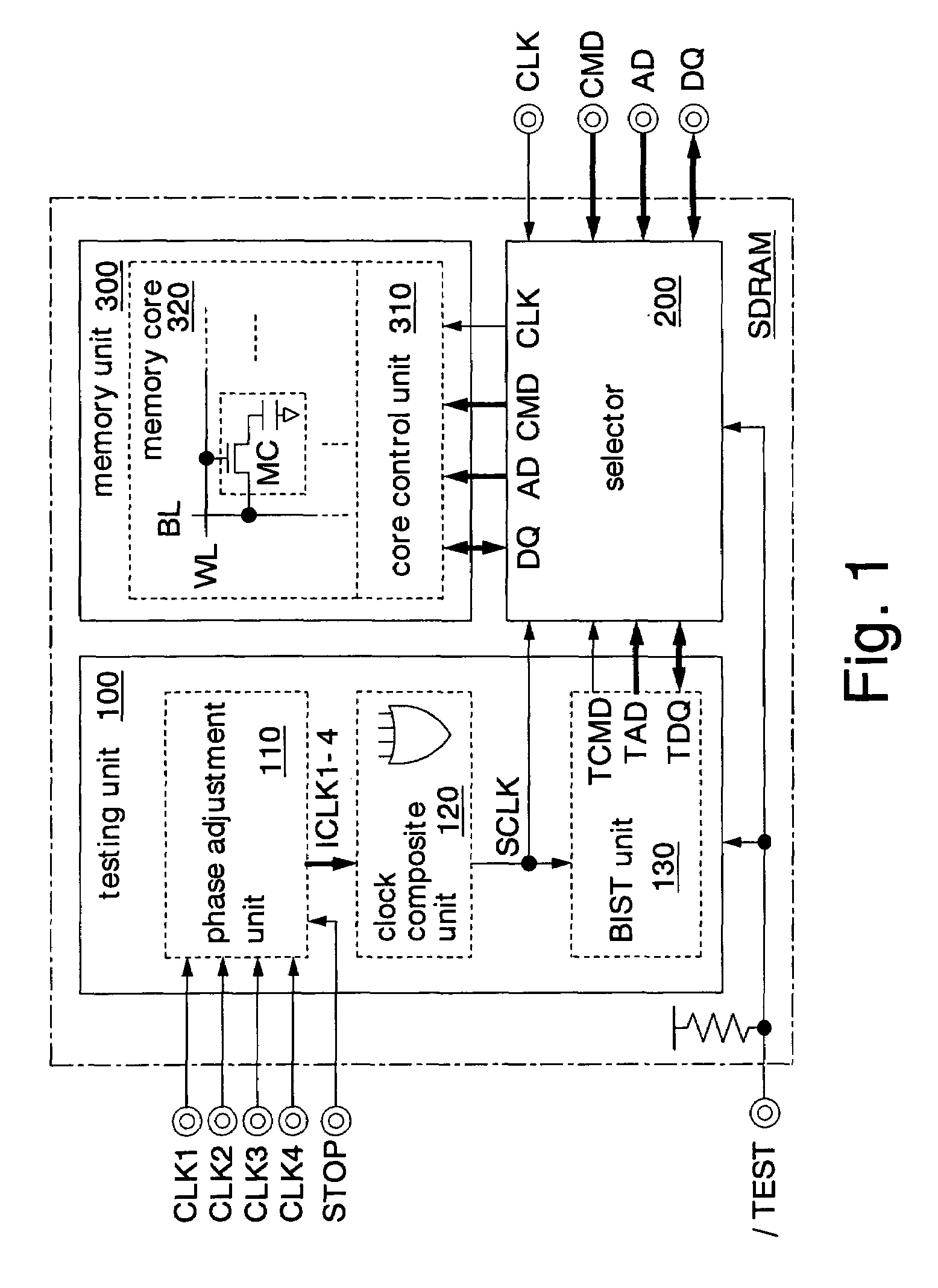
[0054]FIG. 1 shows a first embodiment of the semiconductor integrated circuit of the present invention. This semiconductor integrated circuit is formed on a silicon substrate by using CMOS processes, as a synchronous DRAM (hereinafter, referred to as SDRAM) of clock synchronous type.

[0055]The SDRAM has a testing unit 100, a selector 200, and a memory unit 300 (internal circuit). The testing unit 100 includes a phas...


PUM


Abstract

A phase adjustment unit adjusts the phases of a plurality of external clocks successively shifted in phase, thereby generating a plurality of internal clocks having an equal phase difference between every adjacent transition edges thereof. The internal clocks are synthesized to generate a composite clock having equal pulse intervals. Thus, even when the semiconductor integrated circuit is supplied with external clocks of lower frequencies, it is possible to operate the semiconductor integrated circuit at high speed. For example, the internal circuit can be operated and tested at high speed by using a low-cost LSI tester having a low clock frequency. This can reduce the testing cost of the semiconductor integrated circuit, allowing a reduction in chip cost.

Description

CROSS REFERENCE TO RELATED APPLICATION[0001]This application is based upon and claims the benefit of priority from Japanese Patent Application No. 2004-281723, filed on Sep. 28, 2004, the entire contents of which are incorporated herein by reference.BACKGROUND OF THE INVENTION[0002]1. Field of the Invention[0003]The present invention relates to a semiconductor integrated circuit which operates in synchronization with a clock.[0004]2. Description of the Related Art[0005]With the progress of semiconductor processes, the operating frequencies of semiconductor integrated circuits have been increasing year by year. The frequencies of clocks to be supplied to the semiconductor integrated circuits have also been increasing accordingly. To miniaturize systems that implement semiconductor integrated circuits, there has also been developed a technology for laminating a plurality of semiconductor integrated circuit chips in a single package to manufacture an SIP (System in Package). In the SIP...

Claims


Application Information

Patent Timeline
Patent Type & Authority Patents(United States)
IPC IPC(8): H03L7/00G01R31/28G01R31/3183G11C11/401G11C11/407G11C11/4076G11C29/12G11C29/50H03K5/00H03K5/13H03K5/26
CPCG06F1/12H03K5/133H03L7/0818H03L7/0814H03L7/087H03K2005/00058H03K2005/00071H03L7/00G11C11/407H03L7/08
Inventor TOMITA, HIROYOSHI
Owner SOCIONEXT INC
Why Eureka
Try Eureka