
Delay analysis device, delay analysis method, and computer product

a delay analysis and delay analysis technology, applied in the field of delay analysis devices, delay analysis methods, and computer products, can solve the problems of difficult to accurately deal with statistical factors, influence of statistical factors, unrealistic and inaccurate values of circuit delay,

Inactive Publication Date: 2008-01-15
FUJITSU LTD
View PDF13 Cites 9 Cited by
  • Summary
  • Abstract
  • Description
  • Claims
  • Application Information

AI Technical Summary

Benefits of technology

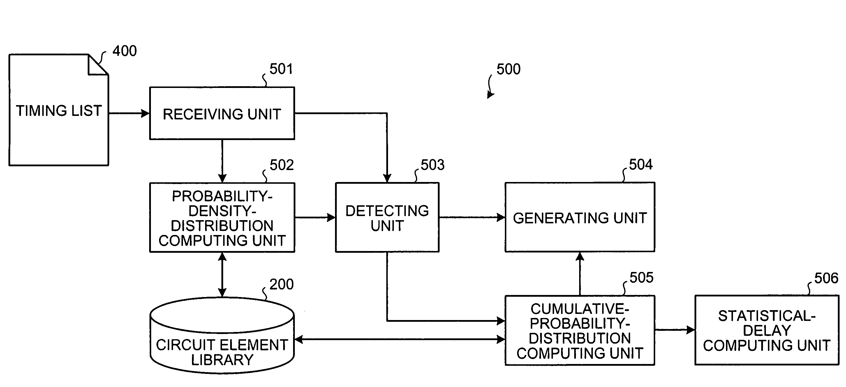
The present invention provides a computer program, a delay analysis device, and a delay analysis method for analyzing circuit delay. The computer program receives a result of a timing analysis of a target circuit and detects critical paths with delays within a predetermined range. The statistical delay of the target circuit is then computed based on a cumulative probability distribution of the delays of the critical paths. This invention helps to improve the accuracy and efficiency of analyzing circuit delay.

Problems solved by technology

Recently, in very large scale integration (VLSI) manufacturing, influence of statistical factors, for example, of process variation, is increasing due to fragmentation of processes.
However, in the conventional technology, it is difficult to accurately deal with statistical factors.
For example, when dealing with statistical factors in a conventional static timing analysis (STA), values of the statistical factors are estimated based on the worst case scenario, thereby resulting in unrealistic and inaccurate values of circuit delay.
This leads to a repetition of circuit designing, thereby increasing the burden on a designer, and causing further delay in designing time.
Carrying out a delay analysis of all paths in a chip by using such conventional technology greatly increases the processing time of the delay analysis, thereby further increasing the designing time.
In other words, because circuit delay is minimized without considering a delay of critical paths, an accurate circuit delay cannot be estimated.

Method used


Image

  • Delay analysis device, delay analysis method, and computer product
  • Delay analysis device, delay analysis method, and computer product
  • Delay analysis device, delay analysis method, and computer product

Examples


Embodiment Construction

[0027]Exemplary embodiments of the present invention will be explained below with reference to accompanying drawings.

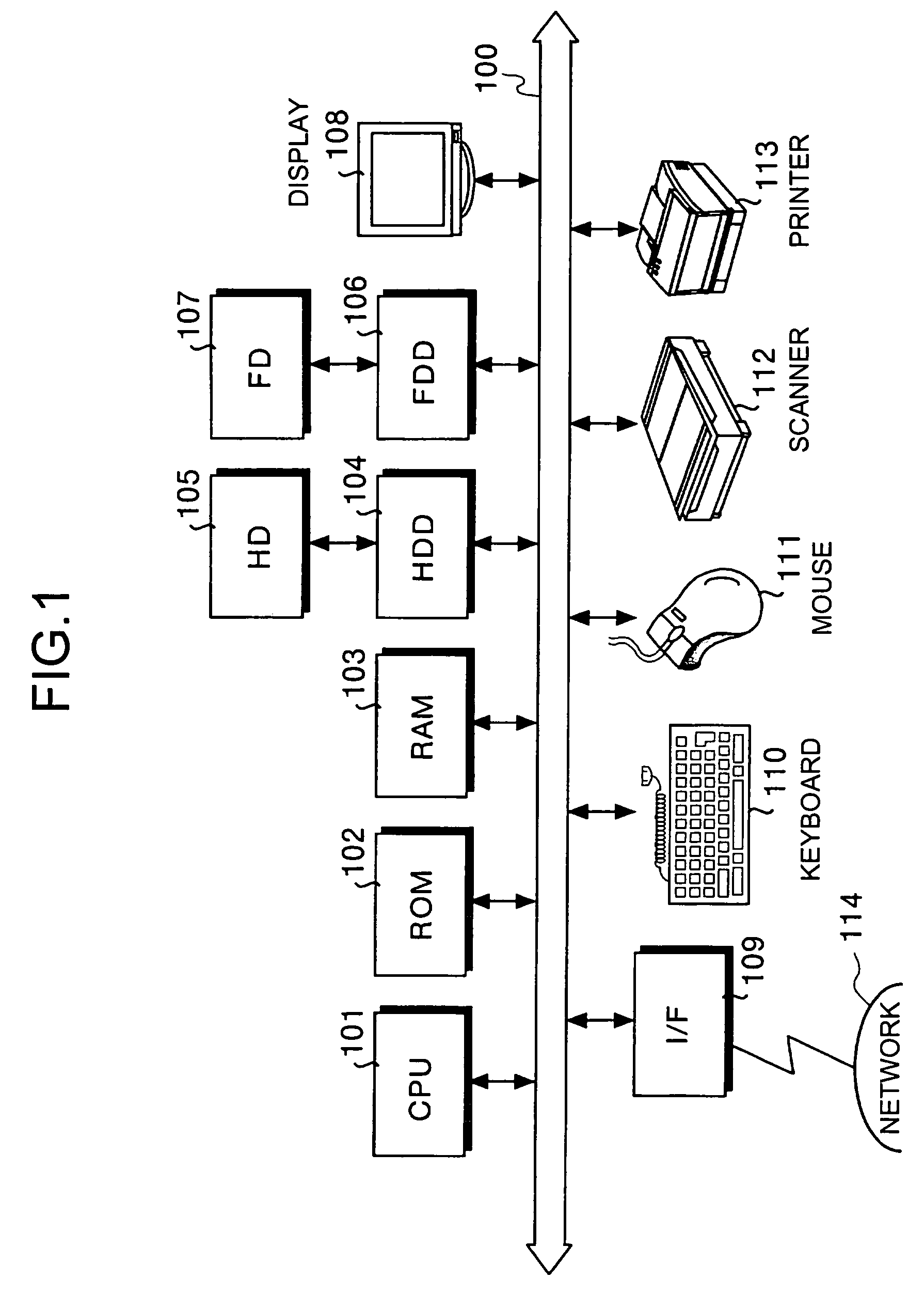
[0028]FIG. 1 is a schematic of a delay analysis device according to an embodiment of the present invention. As shown in FIG. 1, the delay analysis device includes a central processing unit (CPU) 101, a read only memory (ROM) 102, a random access memory (RAM) 103, a hard disk drive (HDD) 104, a hard disk (HD) 105, a flexible disk drive (FDD) 106, a flexible disk (FD) 107 as an example of a removable recording medium, a display 108, an interface 109, a keyboard 110, a mouse 111, a scanner 112, and a printer 113. Paths 100 connect each component.

[0029]The CPU 101 controls the entire delay analysis device. The ROM 102 stores programs such as a boot program. The RAM 103 is used as a work area of the CPU 101. The HDD 104 controls reading of data from and writing of data to the HD 105 according to the control exercised by the CPU 101. The HD 105 stores data that is written a...


PUM


Abstract

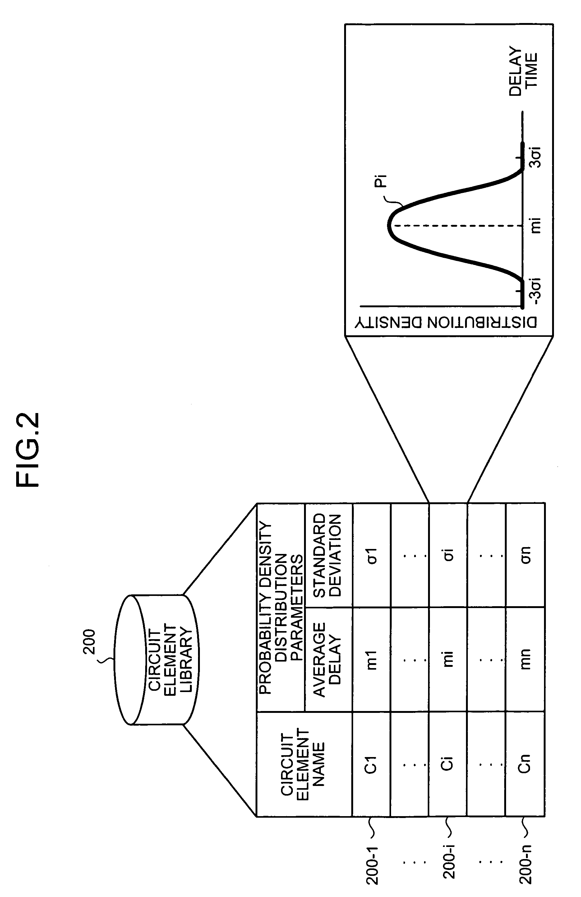
A delay analysis device includes a receiving unit that receives a result of a timing analysis of a target circuit to be analyzed, a detecting unit that detects critical paths having delays within a predetermined range, a statistical-delay computing unit that computes a statistical delay of the target circuit based on a cumulative probability distribution of the delays of the critical paths, and a probability-density-distribution computing unit that computes a probability density distribution of delay of a critical path that has the greatest delay in the result. The detecting unit detects x number of critical paths having cumulative delays within computed probability density distribution.

Description

CROSS-REFERENCE TO RELATED APPLICATIONS[0001]This application is based upon and claims the benefit of priority from the prior Japanese Patent Application No. 2005-278763, filed on Sep. 26, 2005, the entire contents of which are incorporated herein by reference.BACKGROUND OF THE INVENTION[0002]1. Field of the Invention[0003]The present invention relates to a technology for analyzing delay occurring of a circuit.[0004]2. Description of the Related Art[0005]Recently, in very large scale integration (VLSI) manufacturing, influence of statistical factors, for example, of process variation, is increasing due to fragmentation of processes. A technology for decreasing delay considering the influence of statistical factors is required in VLSI designing to obtain high yield in creating circuits that have required performance. Conventionally, a statistical delay analysis method is developed that considers process variation and eliminates unnecessary delay margin (for example, Japanese Patent L...

Claims


Application Information

Patent Timeline
Patent Type & Authority Patents(United States)
IPC IPC(8): G06F17/50
CPCG06F17/504G06F2217/84G06F30/3323G06F2119/12
Inventor HOMMA, KATSUMISHIBUYA, TOSHIYUKIMATSUOKA, HIDETOSHINITTA, IZUMI
Owner FUJITSU LTD
Learn More