Method of reliably electroless-plating integrated circuit die

Active Publication Date: 2008-01-22
NATIONAL SECURITY AGENCY
View PDF7 Cites 18 Cited by
  • Summary
  • Abstract
  • Description
  • Claims
  • Application Information

AI Technical Summary

Benefits of technology

[0013]It is another object of the present invention to uniformly and reliably plate bond pads on individual integrated circuit die for accepting flip-chip solder bumps by eliminating the voltage difference problem between bond

Problems solved by technology

Since an integrated circuit may require a large number of bond wires, serial wire-bonding slows data propagation and is susceptible to high defect rates.
A problem with the prior art methods is not so much in the materials that are used but how the materials are used.
Present methods that u

Method used


Image

  • Method of reliably electroless-plating integrated circuit die
  • Method of reliably electroless-plating integrated circuit die

Examples


Embodiment Construction

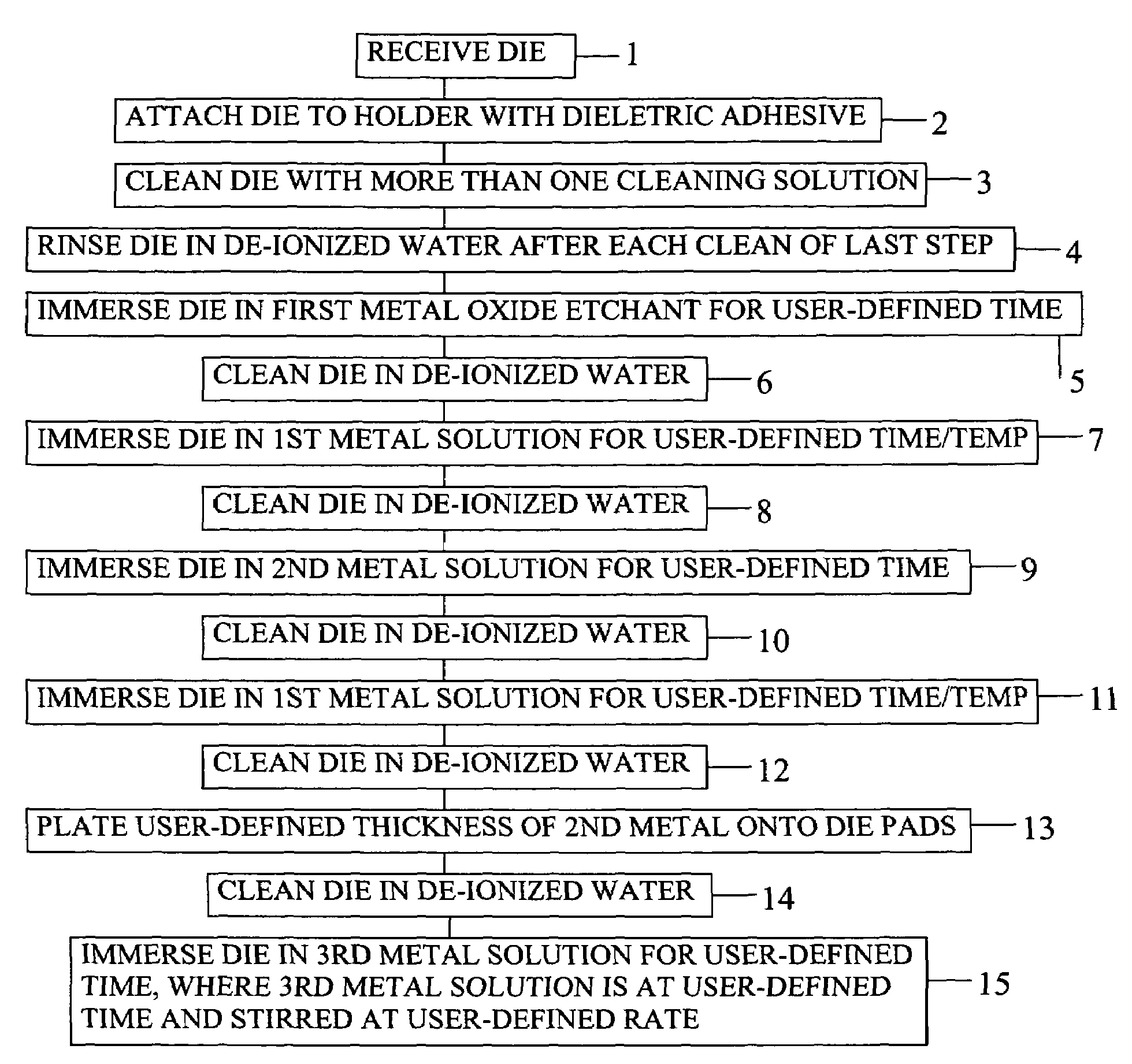
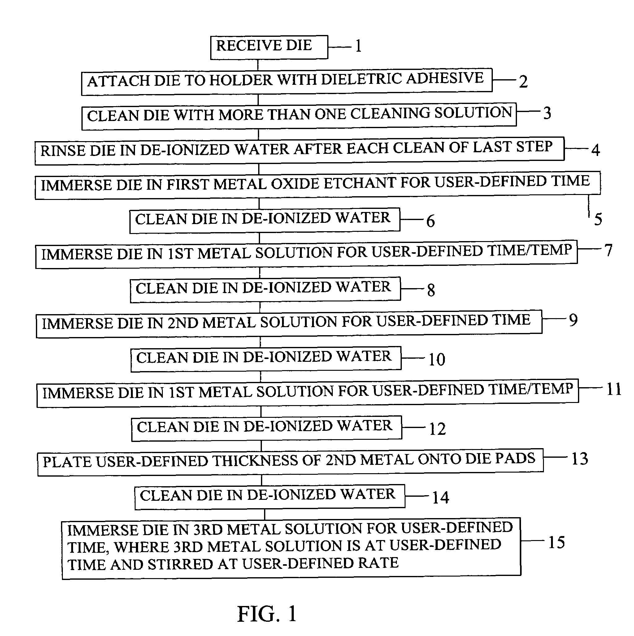
[0032]The present invention is a reliable method of plating bond pads on individual integrated circuit die for accepting solder bumps. The Highly Accelerated Stress Test (HAST) at 135 degrees Centigrade with 95% Relative Humidity, for 1000 hours, was performed on die processed with the present method and yields from 96% to 98% were achieved. The reasons for such success include elimination of any voltage difference between pads on the die, aggressive cleaning steps with multiple cleaning solutions, tight tolerances on solution temperatures, and the use of a heated de-ionized water rinsing step, and so on. The steps of the method are listed in FIG. 1.

[0033]The first step 1 of the method is receiving at least one integrated circuit die. Each integrated circuit die has a pad side and a backside. Typically, the pads are made of aluminum. The present method is designed for aluminum pads, but it may be adapted for pads of any metal with metal specific chemicals.

[0034]The second step 2 of ...


PUM


Abstract

The present invention is a reliable method of electroless-plating integrated circuit die that achieves high yield. Die are attached to a holder using a polyimide adhesive to eliminate voltage differences on bond pads which would otherwise interfere with the plating. The die are aggressively cleaned using multiple cleaning solutions, one heated to a user-defined temperature. Each cleaning is followed by an aggressive rinse in de-ionized water. Die are immersed into multiple metal solutions at user-definable temperatures. Each immersion is followed by an aggressive rinse in de-ionized water, one with heated de-ionized water.

Description

FIELD OF THE INVENTION[0001]The present invention pertains to semiconductor device manufacturing process and, more particularly, flip-chip-type assembly.BACKGROUND OF THE INVENTION[0002]Integrated circuits have become affordable and widely used because of at least two economies of scale in the semiconductor device manufacturing process. The first is the density at which electrical components can be fabricated into an integrated circuit. The second is the number of integrated circuits that may be fabricated at one time on a semiconductor wafer. Integrated circuits fabricated on a semiconductor wafer are then separated, by dicing, and packaged.[0003]The typical packaging technique is to package one integrated circuit at a time using wires individually bonded to each conductive input and output pad of an integrated circuit. Since an integrated circuit may require a large number of bond wires, serial wire-bonding slows data propagation and is susceptible to high defect rates. A packagin...

Claims


Application Information

Patent Timeline
IPC IPC(8): H01L21/44
CPCH01L24/11H01L2224/13099H01L2924/01011H01L2924/01013H01L2924/01015H01L2924/0103H01L2924/01046H01L2924/01078H01L2924/01079H01L2924/14H01L2924/01005H01L2924/01006H01L2924/01019H01L2924/014
Inventor PAL, RATHINDRA N.BERLIN, KINGSLEY R.
Owner NATIONAL SECURITY AGENCY
Why Eureka
Try Eureka