Wiring board having connecting wiring between electrode plane and connecting pad

a wiring and electrode plane technology, applied in the field of wiring boards, can solve the problems of inability to deal with lsi, increase the cost, and expose signal wiring, and achieve the effect of reducing the inductance between the lsi chip and the power supply or ground plane, excellent signal property, and sufficient capability of the chip capacitor

Inactive Publication Date: 2008-01-22
NEC CORP +1
View PDF7 Cites 14 Cited by
  • Summary
  • Abstract
  • Description
  • Claims
  • Application Information

AI Technical Summary

Benefits of technology

[0018]The present invention has been designed to overcome the aforementioned shortcomings of the related art. It is therefore an object of the present invention to provide a semiconductor integrated circuit package that is highly effective for decreasing the switching noise and the signal property thereof is excellent when mounting an LSI of area-array structure.
[0021]With the wiring board of the present invention, it is possible to continuously flow the return current, which is generated on the power supply or ground plane formed on the surface layer, to the LSI chip, even in the case of mounting the LSI of an area-array structure. Thus, the excellent signal property can be maintained. Further, with the wiring board of the present invention, the inductance between the LSI chip and the power supply or ground plane can be decreased. With this, it enables to sufficiently realize the effect of absorbing the switching noise by the power supply or ground plane formed on the surface layer. Moreover, when a chip capacitor for noise absorption is mounted on the surface layer, the capability of this chip capacitor can be sufficiently realized.

Problems solved by technology

It is not possible to deal with the LSI with a large number of pins by a peripheral arrangement in which bumps are disposed only in the peripheral part of the connecting surface.
Thus, it increases the number of wiring layers for enclosing signal wirings that connect the FC pads and BGA (ball grid array) land, thereby increasing the cost.
However, if the signal wiring is disposed on the first layer, the signal wiring is to be exposed.
Therefore, the electric property may be deteriorated.
Therefore, there generates mismatch in the characteristic impedance, thereby causing reflection of the signal or unnecessary radiation.

Method used


Image

  • Wiring board having connecting wiring between electrode plane and connecting pad
  • Wiring board having connecting wiring between electrode plane and connecting pad
  • Wiring board having connecting wiring between electrode plane and connecting pad

Examples


first embodiment

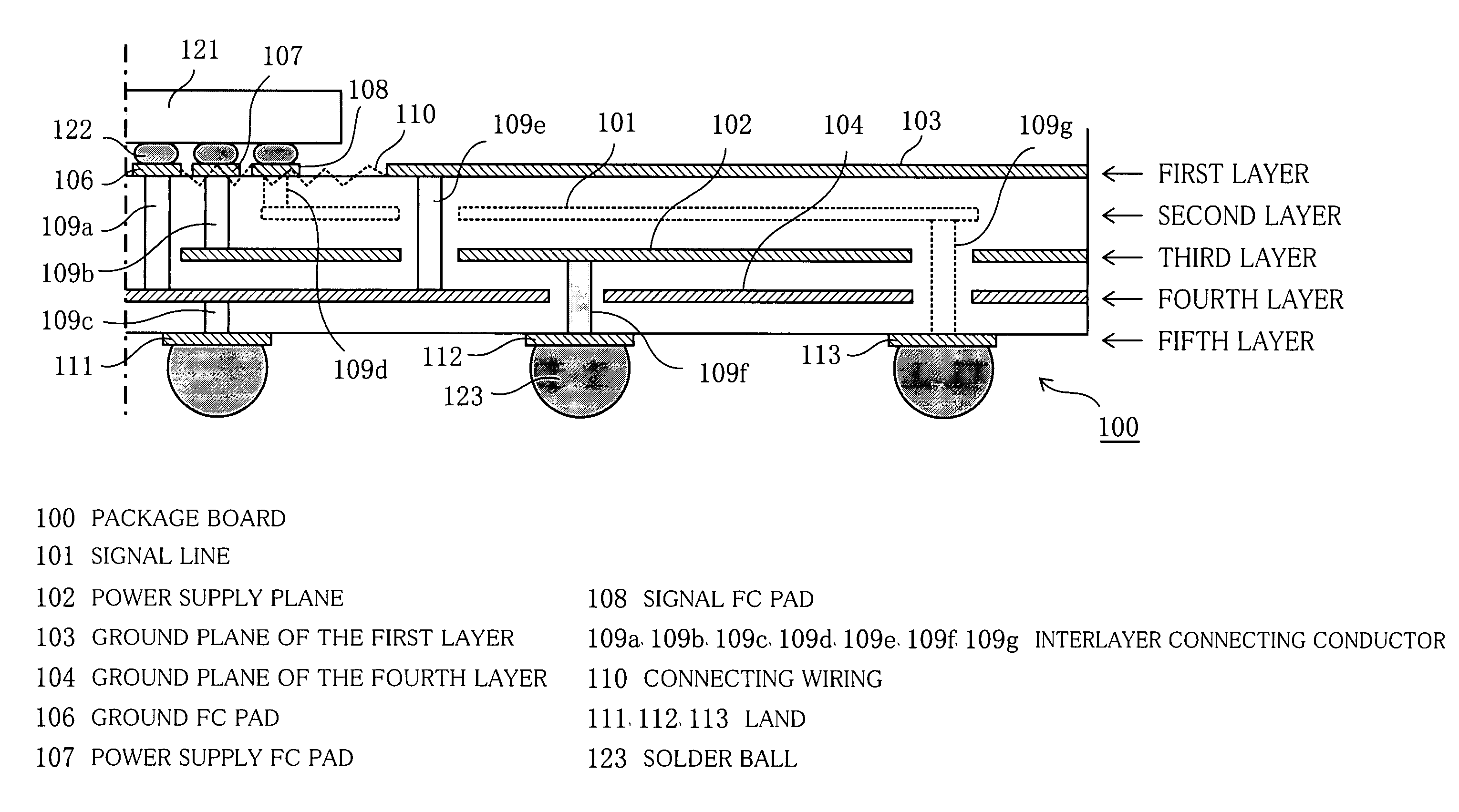
[0046]FIG. 7 is a cross section of the semiconductor integrated circuit package according to a first embodiment of the present invention. The basic structure is the same as the package board of the conventional case shown in FIG. 2. A semiconductor package board 100 is a substrate comprising five wiring layers. The first layer to which an LSI chip is mounted is provided with FC pads 106-108 and a ground plane 103 for mounting the LSI. The second layer is provided with a signal line 101, the third layer with a power supply plane 102, the fourth layer with a ground plane 104, and the fifth layer with lands 111-113 for disposing a solder ball 123. A power supply FC pad 107 of the first layer is connected to the power supply plane 102 of the third layer through an interlayer connecting conductor 109b, and a signal FC pad 108 is connected to the signal line 101 of the second layer through an interlayer connecting conductor 109d. The ground FC pad 106 of the first layer is connected to th...

second embodiment

[0055]Next, a second embodiment of the present invention will be described. This embodiment regards to a semiconductor package in which a chip capacitor is mounted next to the LSI chip. The package board of this embodiment is constituted with five wiring layers. FIG. 14 shows the top plan view of the first layer. In addition, the second to fifth layers of this embodiment are the same as those of the package board of the first embodiment.

[0056]In FIG. 14, the pattern of FC-pad forming part B is the same as that of the first embodiment except that the ground FC pads 106 are formed in consecutive conductive patterns. Thus, it has almost the same functions so that the description thereof will be omitted. In FIG. 14, reference numeral 114 is a power-supply-side pad for mounting the chip capacitor, which is provided by being insulated from the ground plane 103 in an opening formed on the ground plane 103, and 115 is a ground-side pad for mounting the chip capacitor, which is provided on t...

third embodiment

[0060]Next, a third embodiment of the present invention will be described. In the first embodiment, for the connecting wiring, there is used a wiring with uniform wiring width that is the same width as that of the signal wiring. However, the type of the connecting wiring is not limited to this. It may be in any forms as long as it is in a wiring pattern that has a function of electrically connecting the ground FC pads and the ground plane formed around thereof or the power supply FC pads and the power supply plane around thereof. This embodiment illustrates the case where a plane-type wiring is used as the connecting wiring but not the type of signal wiring used in the first embodiment.

[0061]The package board of this embodiment is the package board of the first embodiment but with a modified first layer, in which the pattern forms of the second to fifth layer and the arrangement / shape of the via hole are the same as the case of the first embodiment. FIG. 17 shows the top plan view o...


PUM


Abstract

It is to provide a wiring board for a semiconductor integrated circuit package, which exhibits an excellent signal property and a high effect for decreasing the switching noise at the time of mounting an LSI of an area-array structure. In a multilayer wiring board for a package, which comprises, on a wiring layer of an LSI chip mount surface, a ground pad, a power supply pad, and a signal pad for mounting LSI chip, and a ground plane that extends around a group of those pads, the ground pad disposed on the inner side, among the above-described pads, is connected to the ground plane that surrounds the pad group through a connecting wiring.

Description

BACKGROUND OF THE INVENTION[0001]1. Field of the Invention[0002]The present invention relates to a wiring board for a semiconductor integrated circuit package and a semiconductor integrated circuit device using the wiring board. Particularly, it relates to a wiring board for a semiconductor integrated circuit package for mounting an LSI chip by flip-chip connection and to a semiconductor integrated circuit device in which an LSI chip is mounted on the wiring board.[0003]2. Description of the Related Art[0004]Recently, the number of pins and the frequency of an LSI have been increased. Accordingly, when forming an LSI package, there is a technique that is broadly used for flip-chip connecting the LSI to a package board. FIG. 1 is a plan view for showing an example of a connecting surface of an LSI between a package, which has bumps arranged in an area-array form. It is not possible to deal with the LSI with a large number of pins by a peripheral arrangement in which bumps are dispose...

Claims


Application Information

Patent Timeline
Patent Type & Authority Patents(United States)
IPC IPC(8): H01L23/12
CPCH01L23/49822H01L23/50H05K1/0218H01L23/49838H01L2224/16235H01L2924/01057H01L2924/01078H01L2924/09701H01L2924/15173H01L2924/15174H01L2924/15311H01L2924/19105H01L2924/3011H01L2924/3025H05K1/0219H05K1/0231H05K1/0298H05K1/112H05K2201/0715H01L2224/16225H01L2924/00011H01L2924/00014H01L2224/0401
Inventor SAKAI, JUNINOUE, HIROBUMIMOTONAGA, KAZUHIRO
Owner NEC CORP
Why Eureka
Try Eureka