

Substrate treating apparatus
a technology for treating apparatus and substrates, applied in the direction of instruments, photosensitive materials, furnaces, etc., can solve the problems of unused space perpendicular to directions, affecting the nozzle, and not being able to receive prompt heating treatment of exposed substrates, etc., and achieve the effect of efficiently transferring substrates
- Summary
- Abstract
- Description
- Claims
- Application Information
AI Technical Summary
Benefits of technology
Problems solved by technology
Method used
Image

Examples
first embodiment
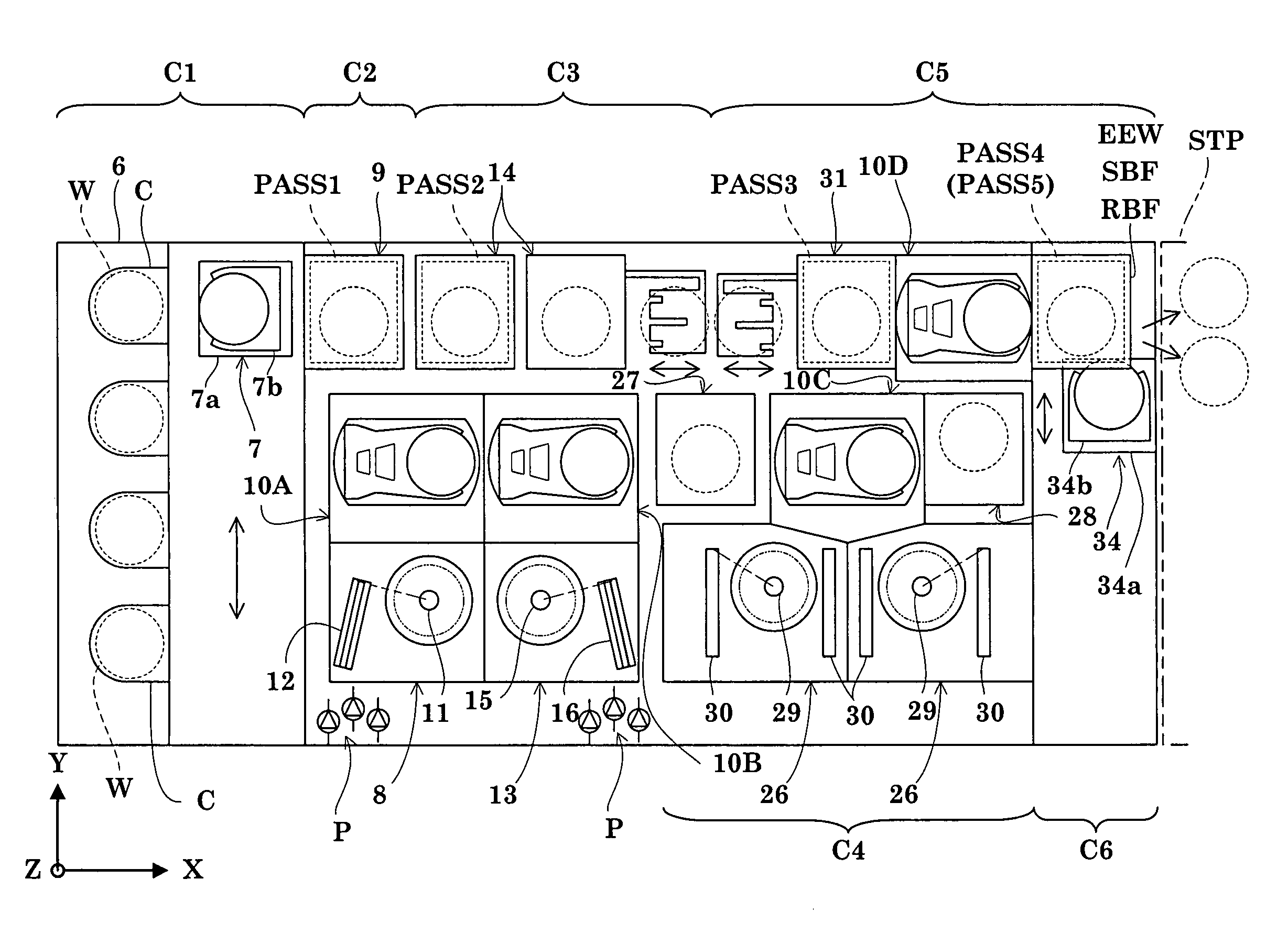
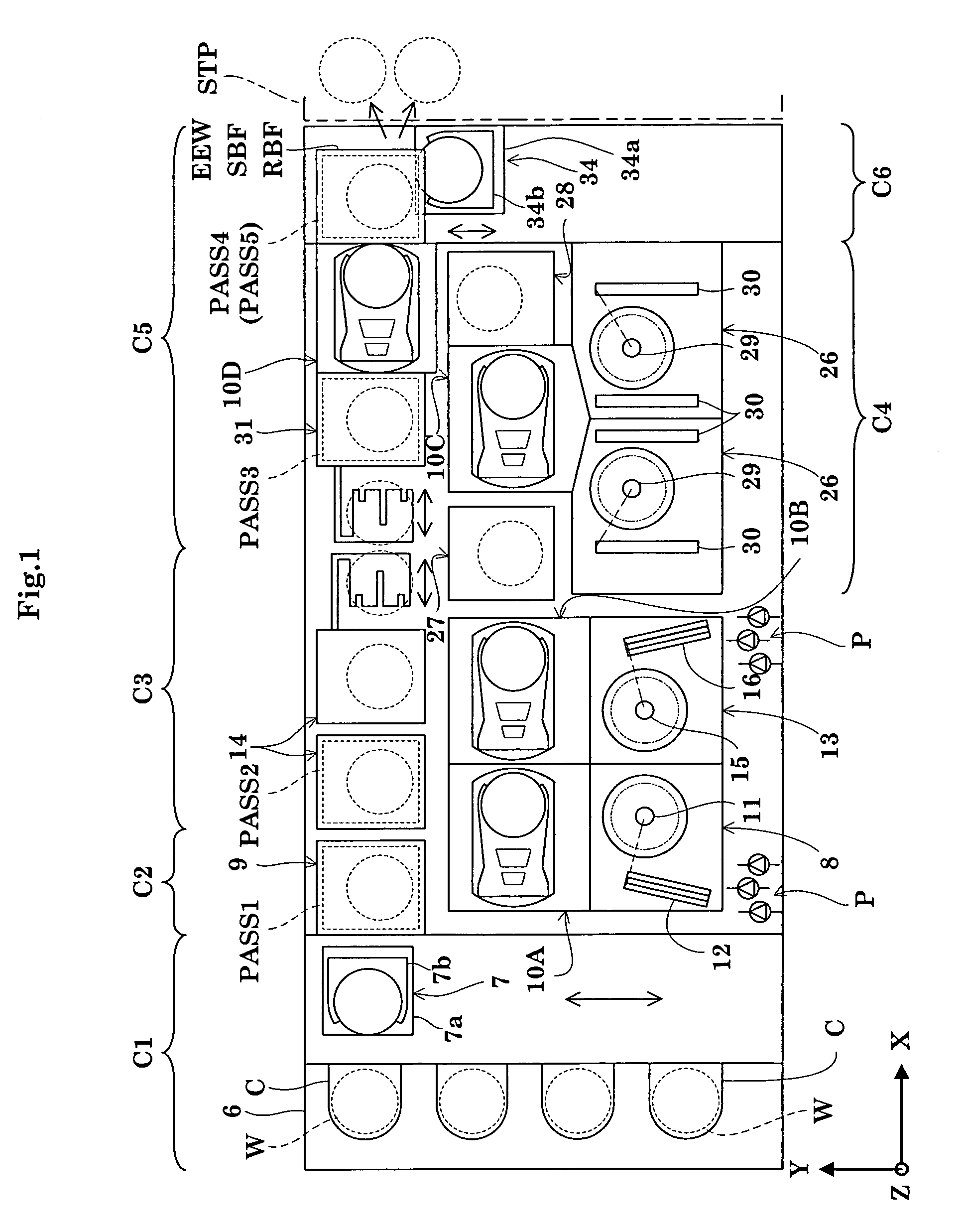
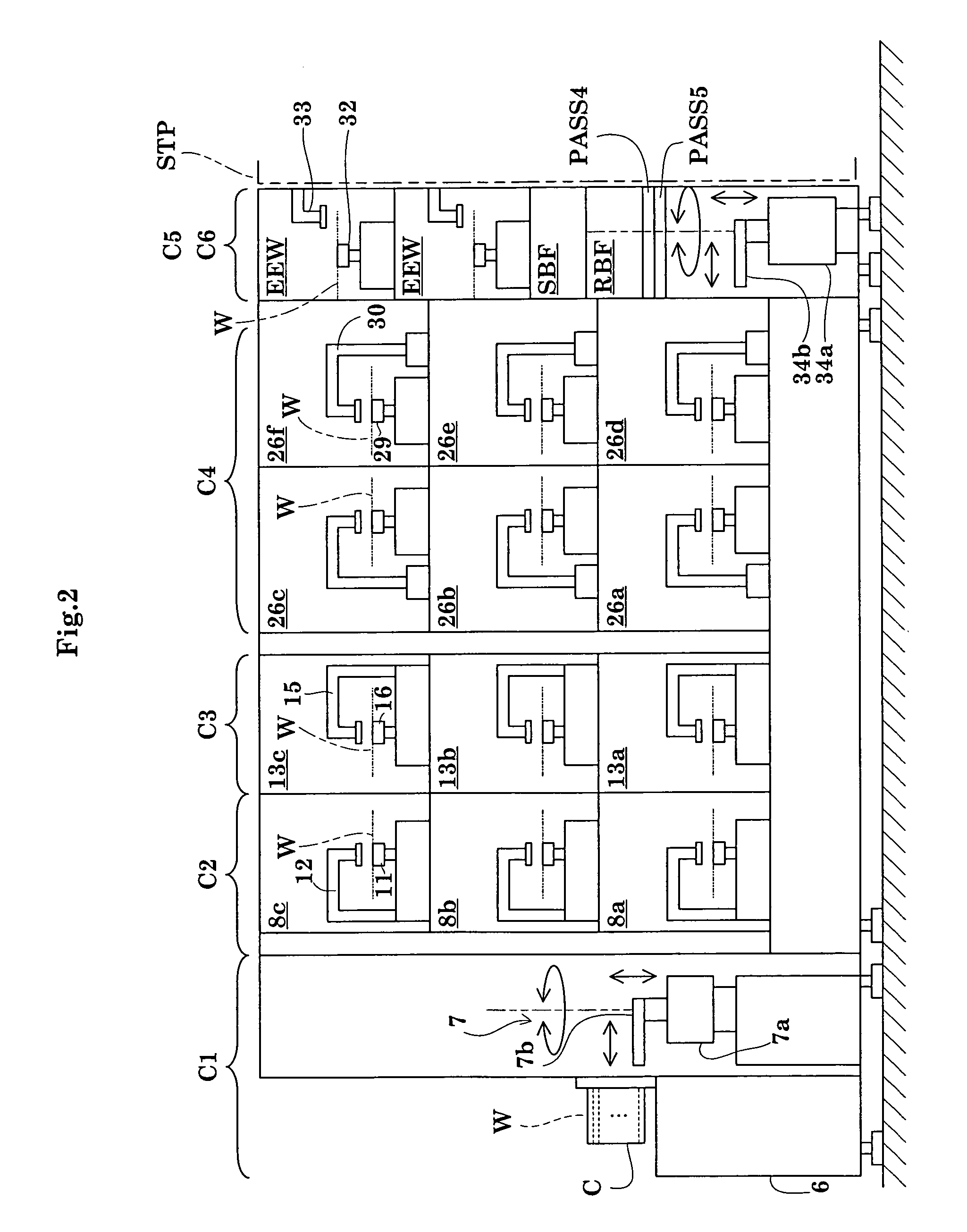
[0068]FIG. 1 is a plan view showing an outline of a substrate treating apparatus in a first embodiment. FIG. 2 is a front view showing an outline of the apparatus in the first embodiment. FIG. 3 is a front view of heat-treating modules.
[0069]The illustrated apparatus is a substrate treating apparatus constructed to perform chemical treatment for forming antireflection film and photoresist film on semiconductor wafers (hereinafter called simply “substrates or wafers”) and developing exposed substrates. The substrates handled by the substrate treating apparatus according to this invention are, of course, not limited to semiconductor wafers, but include various substrates such as glass substrates for liquid crystal displays. The chemical treatment is not limited to formation of photoresist film or the like or development, but includes various other chemical treatments.
[0070]The substrate treating apparatus in the first embodiment includes an indexer cell C1 for fetching wafers W from c...
second embodiment
[0151]Next, the second embodiment of this invention will be described with reference to the drawings.
[0152]FIG. 12 is a plan view of a substrate treating apparatus in the second embodiment. FIG. 13 is a front view thereof. FIG. 14 is a front view of heat-treating modules. FIG. 15 is a plan view showing an arrangement of cells in the apparatus. FIG. 16 is a view showing flows of substrate transport by first to fourth main transport mechanisms.
[0153]The substrate treating apparatus in the second embodiment has cells C1-C6 arranged as shown in FIGS. 12 and 15.
[0154]The antireflection film forming cell C2 in the second embodiment includes antireflection film coating modules 8, two groups of antireflection film heat-treating modules 9, and a first main transport mechanism 10A. The antireflection film coating modules 8 and one group of antireflection film heat-treating modules 9 are opposed to each other across the first main transport mechanism 10A. The other group of antireflection film...
third embodiment
[0166]Next, the third embodiment of this invention will be described with reference to the drawings.
[0167]FIG. 17 is a plan view of a substrate treating apparatus in the third embodiment. FIG. 18 is a front view thereof. FIG. 19 is a front view of heat-treating modules. FIG. 20 is a plan view showing an arrangement of cells in the apparatus. FIG. 21 is a view showing flows of substrate transport by first to fourth main transport mechanisms.
[0168]The substrate treating apparatus in the third embodiment has cells C1-C6 arranged as shown in FIGS. 17 and 20.
[0169]The antireflection film forming cell C2 in the third embodiment includes antireflection film coating modules 8, two groups of antireflection film heat-treating modules 9, and a first main transport mechanism 10A. The antireflection film coating modules 8 and one group of antireflection film heat-treating modules 9 are opposed to each other across the first main transport mechanism 10A. The other group of antireflection film hea...
PUM
| Property | Measurement | Unit |
|---|---|---|
| time | aaaaa | aaaaa |
| temperature | aaaaa | aaaaa |
| viscosity | aaaaa | aaaaa |
Abstract
Description
Claims
Application Information