Bipolar transistor and semiconductor device using same

a technology of bipolar transistors and semiconductor devices, applied in semiconductor devices, semiconductor/solid-state device details, electrical apparatus, etc., can solve the problems of increasing the size of transistors and incurring the increase of the number of processes of npn transistors, and achieve the effect of reducing the number of processes and small in siz

Inactive Publication Date: 2008-01-29
ROHM CO LTD
View PDF5 Cites 0 Cited by
  • Summary
  • Abstract
  • Description
  • Claims
  • Application Information

AI Technical Summary

Benefits of technology

[0009]It is an object of the present invention to provide a bipolar transistor which is low in collector-to-emitter saturation voltage, small in size and to be manufactured by the reduced number of processes, and a semiconductor device formed with such a bipolar transistor and a MOS transistor on a same substrate.
[0011]This high concentration region is formed in a manner substantially surrounding an entire periphery of the base region, in which can lower the collector-to-emitter saturation voltage without the necessity of forming in such a depth as reaching the buried layer as required in the collector wall of the related-art bipolar transistor, thereby making it possible to reduce the spread in a lateral direction. Accordingly, the bipolar transistor can be made smaller in size than the related art. Also, because the high concentration region can be formed by utilizing the fabrication process for other elements to be formed together with the bipolar transistor on the same substrate, the bipolar transistor can be fabricated through a reduced number of processes by omitting the diffusion process exclusive for forming a high concentration region.
[0013]This high concentration region, because not necessarily to be formed in such a depth as reaching the buried layer as in the collector wall of the related-art bipolar transistor, making it possible to reduce the spread in a lateral direction. Accordingly, the bipolar transistor can be made smaller in size than that of the related art. Also, because the high concentration region can be formed by utilizing the fabrication process for a MOS transistor to be formed together with the bipolar transistor on the same substrate, it is possible to omit the diffusion process exclusive for forming a high concentration region. Consequently, the thermal process for diffusion can be reduced, it is possible to reduce the spread in diffusion length of the already formed diffusion region, making it possible to provide an accurate, reliable semiconductor device. Also, because diffusion process is omitted once, a semiconductor device can be manufactured by smaller number of processes.
[0014]The high concentration region may be formed in the same process as source and drain regions of the MOS transistor. In this manner, by forming a high concentration region for reducing the bipolar-transistor collector-to-emitter saturation voltage in a same process as the source and drain regions for the MOS transistor, the bipolar transistor can be fabricated through a smaller number of processes by omitting the diffusion process exclusive for forming a high concentration region.
[0015]The high concentration region is desirably formed in the same process as regions for countermeasure against breakdown provided in source and drain regions of the MOS transistor. In this manner, by forming a high concentration region for reducing the bipolar-transistor collector-to-emitter saturation voltage in a same process as the source and drain regions for the MOS transistor, the bipolar transistor can be fabricated through a smaller number of processes by omitting the diffusion process exclusive for forming a high concentration region.

Problems solved by technology

This increases spacing between the collector electrode 88 and the base electrode 91, resulting in a problem of increased transistor size.
Thus, there arises a problem of incurring the increase in the number of processes for an NPN transistor 80 and, eventually, a semiconductor device having NPN transistors 80.

Method used


Image

  • Bipolar transistor and semiconductor device using same
  • Bipolar transistor and semiconductor device using same
  • Bipolar transistor and semiconductor device using same

Examples


first embodiment

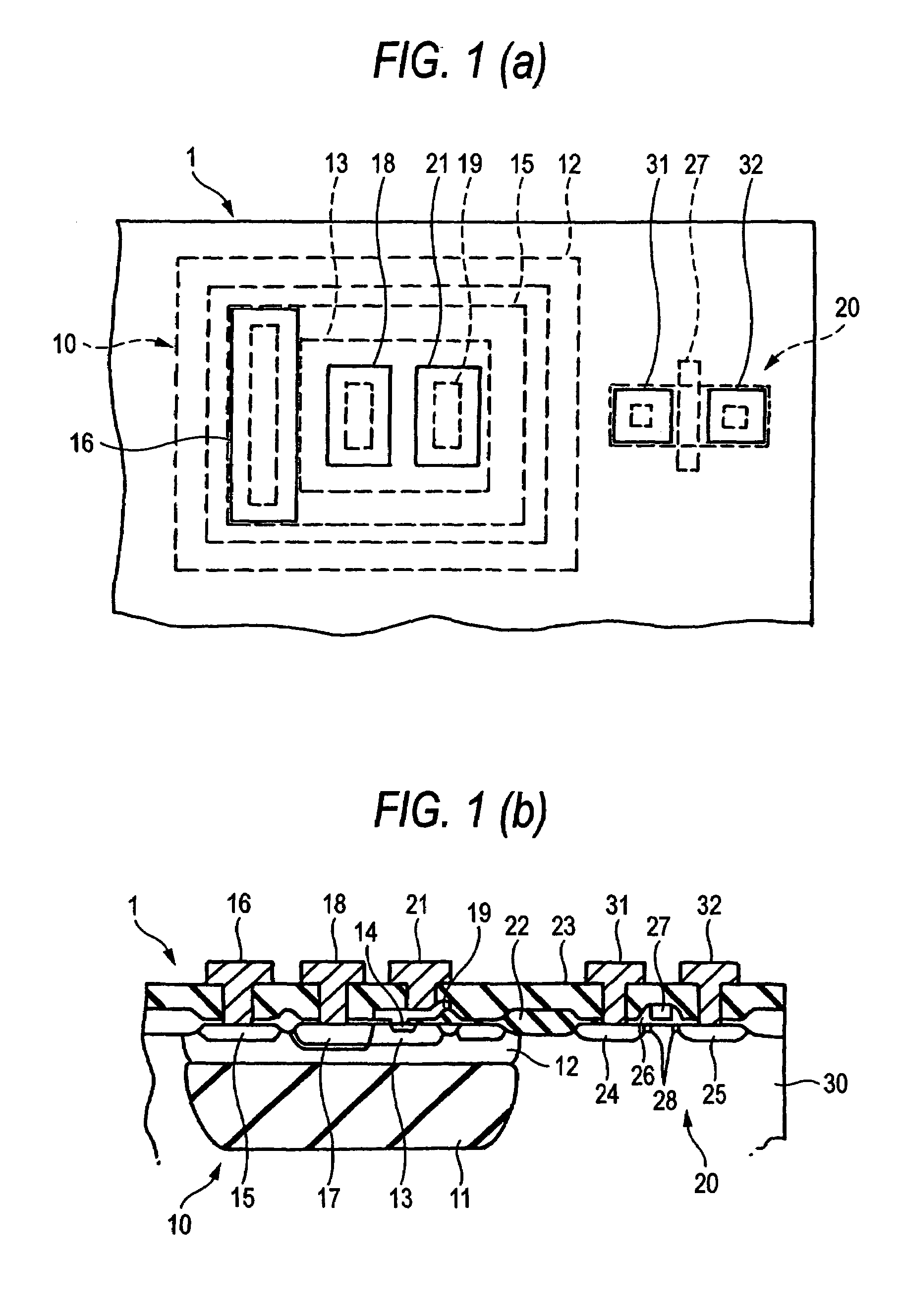
[0025]FIG. 1A is a plan view showing a semiconductor device according to the invention while FIG. 2 is a sectional view of the same. The semiconductor device 1 is formed with an NPN transistor 10 and an NMOS transistor 20 on a same silicon substrate 30.

[0026]The NPN transistor 10 includes an N+ buried layer formed by diffusing As (arsenic), Sb (antimony) or the like to the P-type substrate 30, a collector region 12 formed thereon by an N− layer, a base layer 13 formed by a P− layer in the collector layer 12, and an emitter layer 14 formed by an N layer in the base region 13.

[0027]In the collector region 12, a high concentration region 15 is formed in a manner fully surrounding the entire periphery of the base region 13, in order to reduce the collector-to-emitter saturation voltage VCE(sat). A collector electrode 16 is connected to the high concentration region 15. The high concentration region 15 is an N+ layer diffused with As (arsenic).

[0028]In the base region 13, a base contact ...

second embodiment

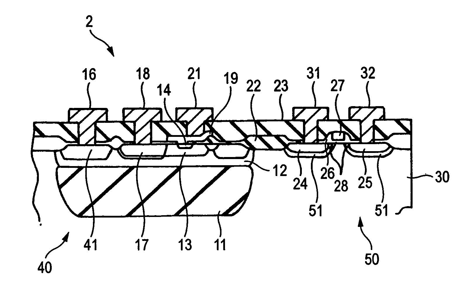
[0034]FIG. 2 is a sectional view showing a semiconductor device according to the invention. The semiconductor device 2 is formed with an NPN transistor 40 and an NMOS transistor 50 on the same silicon substrate 30. The difference from the semiconductor device 1 of FIG. 1 lies in that the high concentration region 41 formed in a collector region 12 of an NPN transistor 40 is formed by an N+ layer diffused with P (phosphorus) greater in diffusion coefficient than As (arsenic) and that the source region 24 and the drain region 25 of the NMOS transistor 50 are formed with respective regions 51, for countermeasure against static breakdown, diffused with P (phosphorus).

[0035]The high concentration region 41 is formed in the same process as in forming the regions 51 for countermeasure against static breakdown for the NMOS transistor 50. Namely, when P (phosphorus) is diffused in the P-type silicon substrate 30 to form N+-layered regions 51 for countermeasure against static breakdown, the c...

third embodiment

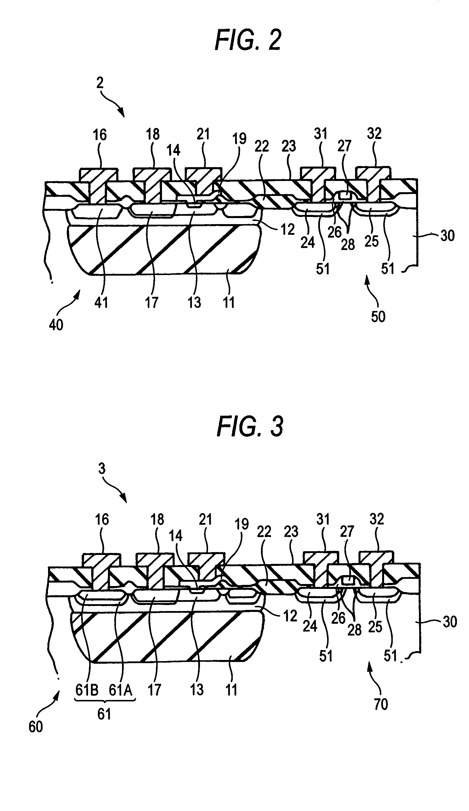
[0037]FIG. 3 is a sectional view showing a semiconductor device according to the invention. The semiconductor device 3 is formed with an NPN transistor 60 and an NMOS transistor 70 on the same silicon substrate 30. The difference from the semiconductor device 2 of FIG. 2 resides in that the high concentration region 61 formed in a collector region 12 of an NPN transistor 60 is formed by an N+-layered first region 61A diffused with P (phosphorus) and an N+-layered second region 61B diffused with As (arsenic).

[0038]The first region 61A of the high concentration region 61 is formed in the same process as in forming the breakdown-countermeasure regions 51 for the NMOS transistor 50, while the second region 61B is formed in the same process as in forming the source region 24 and drain region 25. Namely, when P (phosphorus) is diffused to the P-type silicon substrate 30 to form N+-layered regions 51 for countermeasure against breakdown, the collector region 12 is diffused by P (phosphorus...


PUM


Abstract

A bipolar transistor is provided, which is low in collector-to-emitter saturation voltage, small in size and to be manufactured by a reduced number of processes, and a semiconductor device formed with such a bipolar transistor and a MOS transistor on a same substrate. A high concentration region for reducing the collector-to-emitter saturation voltage VCE(sat) is formed in a manner surrounding a base region of an NPN transistor. This high concentration region is not necessarily formed in such a depth as reaching a buried layer, and can be reduced in the spread in a lateral direction. Because a high concentration region can be formed in a same process as upon forming source and drain regions for an NMOS transistor to be formed together with an NPN transistor on a same silicon substrate, it is possible to omit a diffusion process exclusive for forming a high concentration region and hence to manufacture a semiconductor device through a reduced number of processes.

Description

[0001]This application is a continuation of application Ser. No. 10 / 397,648, filed Mar. 26, 2003, which application is incorporated herein by reference.BACKGROUND OF THE INVENTION[0002]1. Field of the Invention[0003]This invention relates to bipolar transistors and semiconductor devices and, more particularly, to a bipolar transistor lowered in collector-to-emitter saturation voltage VCE(sat) and a semiconductor device formed with such a bipolar transistor and a MOS transistor on a same substrate.[0004]2. Description of the Related Art[0005]There is shown, in FIG. 5, a structure of a semiconductor device in an related art formed with NPN and NMOS transistors on a same substrate. FIG. 5A is a plan view while FIG. 5B is a sectional view of the same.[0006]An NPN transistor 80 includes an N+ buried layer 82 formed of As (arsenic), Sb (antimony) or the like in a P-type silicon substrate 81, a collector region 83 formed thereon by an N−layer, a base region 84 formed by a P−layer in the co...

Claims


Application Information

Patent Timeline
Patent Type & Authority Patents(United States)
IPC IPC(8): H01L29/76H01L21/8222H01L21/331H01L21/8248H01L21/8249H01L27/06H01L29/732
CPCH01L29/7322H01L27/0623
Inventor SAKURAGI, MASAHIRO
Owner ROHM CO LTD
Why Eureka
Try Eureka