

Semiconductor device
a semiconductor and semiconductor technology, applied in semiconductor devices, semiconductor/solid-state device details, electrical devices, etc., can solve the problems of reducing the capacity value affecting the quality so as to achieve the effect of short filling time of the conducting layer, small capacity value, and dramatic reduction of the capacity between the semiconductor substrate and the inner through-electrod
- Summary
- Abstract
- Description
- Claims
- Application Information
AI Technical Summary
Benefits of technology
Problems solved by technology
Method used
Image

Examples
first embodiment
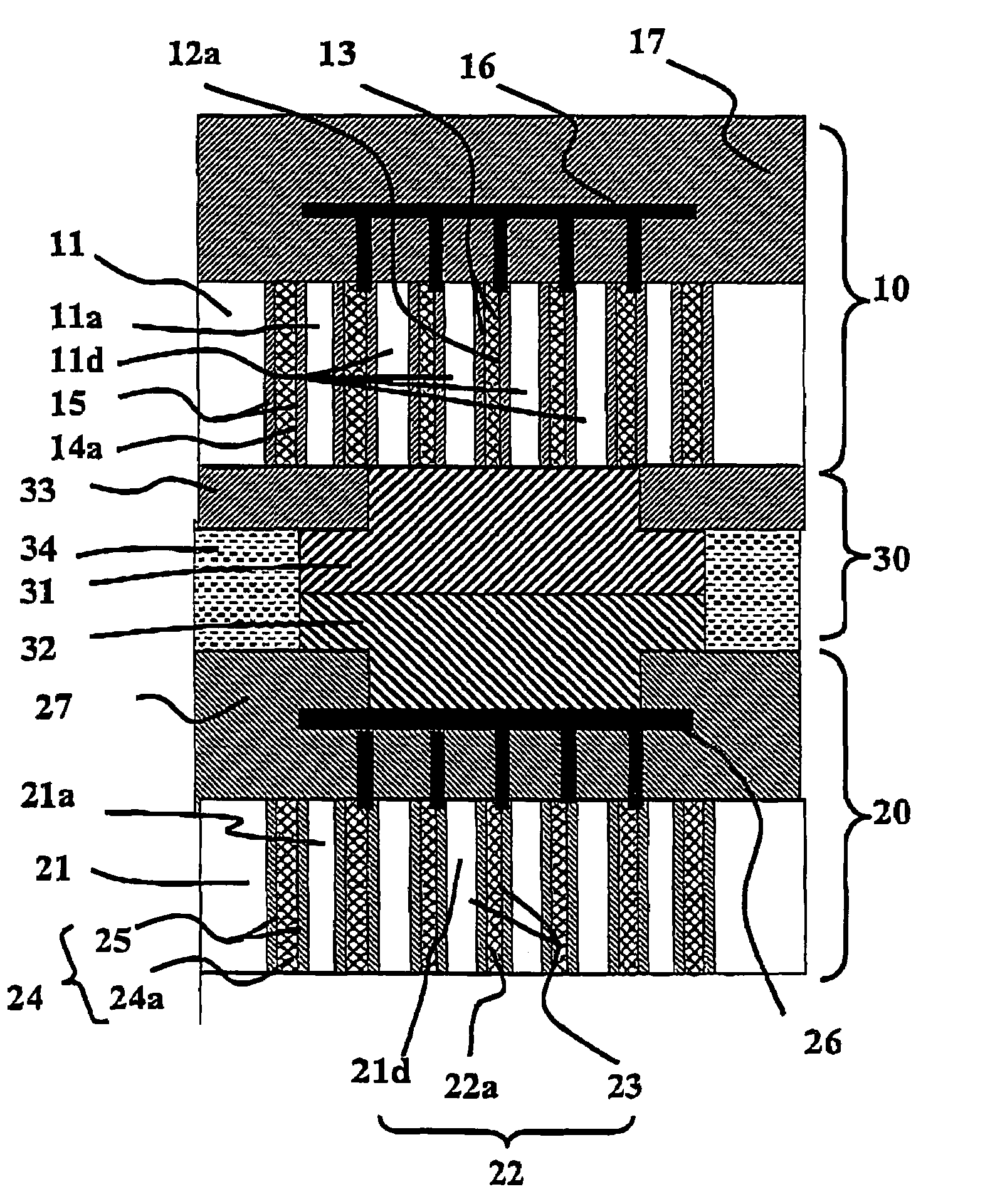
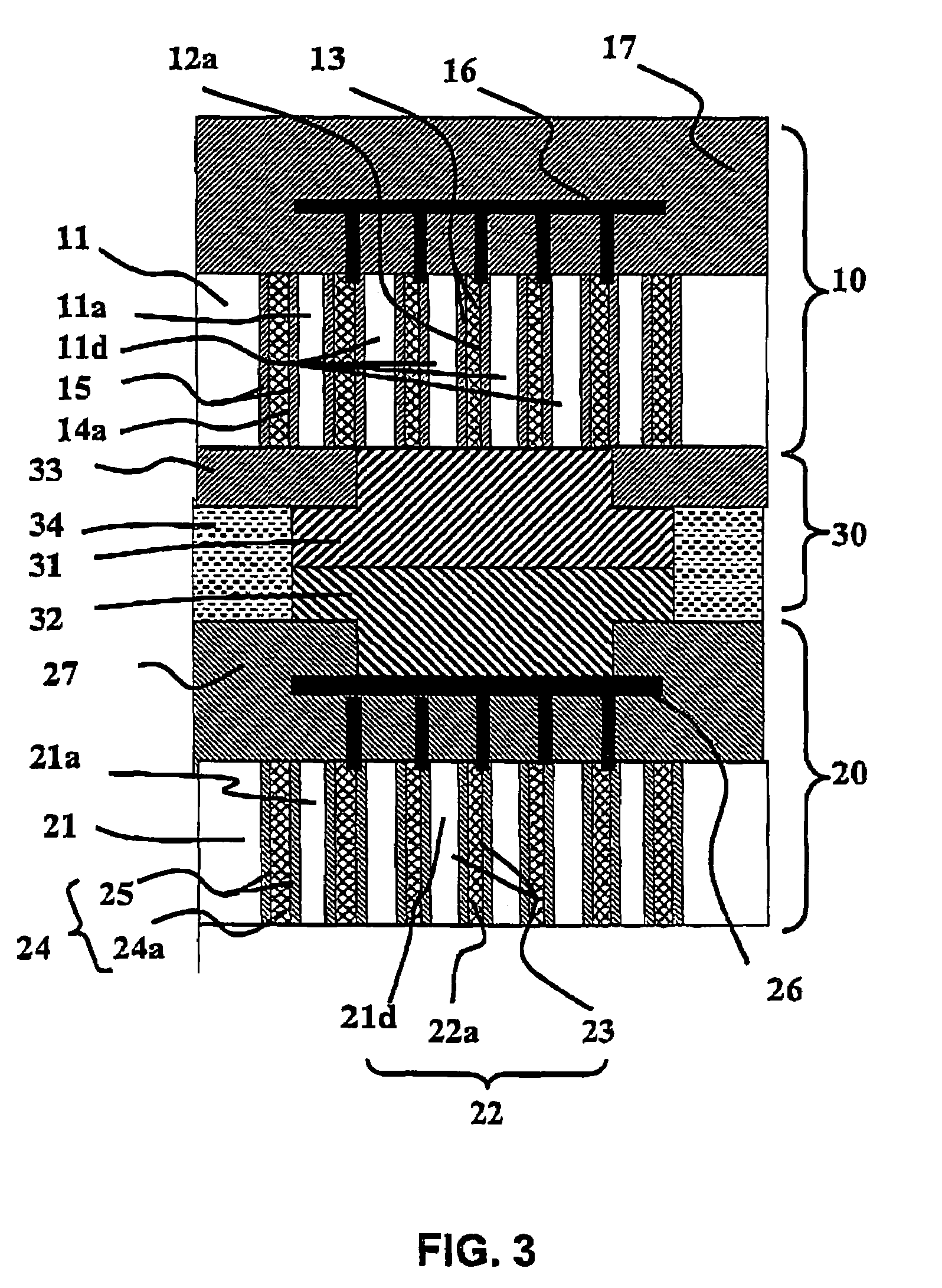
[0058]A three-dimensional semiconductor device according to the present invention will be described as a first embodiment thereof, with reference to FIGS. 3 to 8. Here, FIG. 3 is a sectional view of a three-dimensional semiconductor device according to the present invention. FIG. 4 is a plan view of a through-electrode having an outer peripheral layer in the present invention. FIG. 5 is a plan view of a through-electrode having a dual peripheral layer in the present invention. FIG. 6 is a plan view of another through-electrode having a dual peripheral layer in the present invention. FIG. 7 is a graph showing the dependence of the through-electrode capacity upon the number of outer peripheral layers. FIG. 8 is a graph showing the dependence of the through-electrode capacity upon the thickness of an oxide layer, in the presence and absence of an outer peripheral layer.
[0059]FIG. 3 is a sectional view of a through-electrode connection portion 30 in which a semiconductor chip 10 and a s...
second embodiment
[0075]A production process of the three-dimensional semiconductor device according to the present invention will be described as a second embodiment thereof, with reference to FIGS. 9A to 9c and FIGS. 10A and 10B. Sectional views in FIGS. 9A to 9c and FIGS. 10A and 10B each show one of a plurality of the through-electrodes of the three-dimensional semiconductor device. Herein, the same components as those in the first embodiment are designated by the same reference numerals.
[0076]As shown in FIG. 9A, by applying lithography, etching, and the like to the semiconductor substrate 11, trenches 18 for the inner through-electrode 12 and trenches 19 for the outer through-electrode 14 are formed. Quadrangular ring-shaped semiconductor 11a and columnar semiconductors 11d are formed in the semiconductor substrate 11 by the trenches 18 and the trenches 19. The trenches 18 are formed to have equal widths, and the trenches 19 are formed into a size equal to or smaller than the trenches 18. Equal...
PUM
 Abstract
Description
Claims
Application Information