
Effective I/O ESD protection device for high performance circuits

a protection device and high-performance technology, applied in semiconductor devices, semiconductor/solid-state device details, electrical apparatus, etc., can solve the problems of reducing the trigger voltage of both the pull-down transistor and the logic transistor, and the i/o pull-down transistor may not be able to protect the i/o logic circuit, and achieves the effect of little impact on the junction capacitan

Inactive Publication Date: 2008-02-05
ALTERA CORP
View PDF7 Cites 18 Cited by
  • Summary
  • Abstract
  • Description
  • Claims
  • Application Information

AI Technical Summary

Benefits of technology

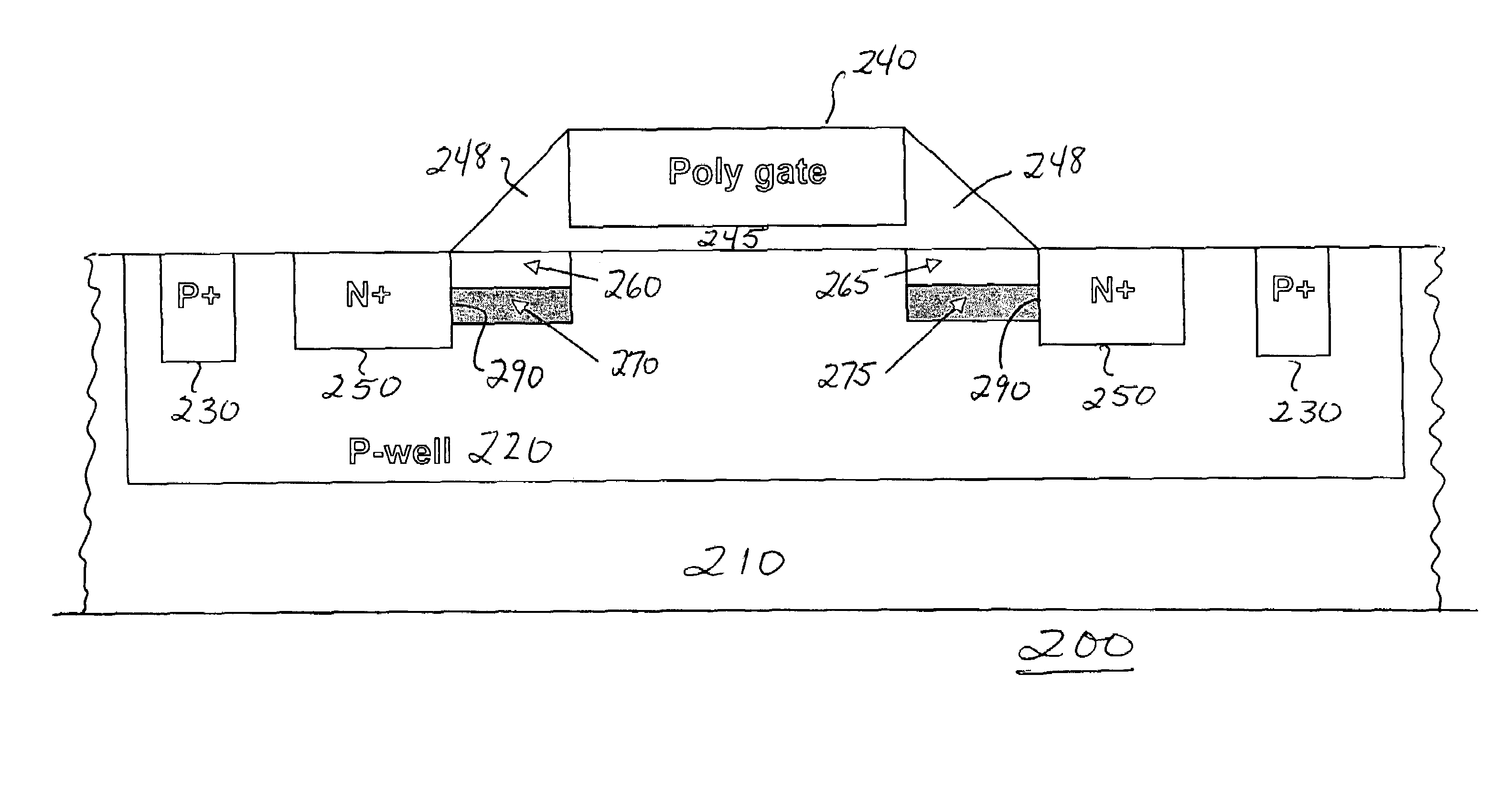
[0006]The mask limits the doping of the second conductivity type to a relatively small region under the lightly doped drain regions with the result that there is very little impact on the junction capacitance. In particular, we have found that if the second doped region is formed under about 25% of the lightly doped drain regions, the junction capacitance does not change by more than 1%. In addition, the mask limits the doping of the second conductivity type to the I / O pull-down transistors so that the I / O logic transistor area in the same integrated circuit does not receive the doping. As a result, the breakdown voltage of the drain / source junction of the I / O logic transistors is not affected.

Problems solved by technology

As device dimensions get smaller and smaller, it becomes increasingly more difficult to use such I / O pull-down devices to protect I / O logic circuits.
However, since the P-type pocket implants are used throughout the circuit, this reduces the trigger voltage of both the pull-down transistors and the logic transistors.
As a result, the I / O pull-down transistor may not be able to protect the I / O logic circuit.
In addition, the P-type pocket implant can degrade the transistor performance by increasing its junction capacitance, and thereby reducing its speed, and can increase the transistor leakage.
This, however, significantly increases the junction capacitance and affects the transistor performance.
It also increases the transistor leakage.

Method used


Image

  • Effective I/O ESD protection device for high performance circuits
  • Effective I/O ESD protection device for high performance circuits
  • Effective I/O ESD protection device for high performance circuits

Examples


Embodiment Construction

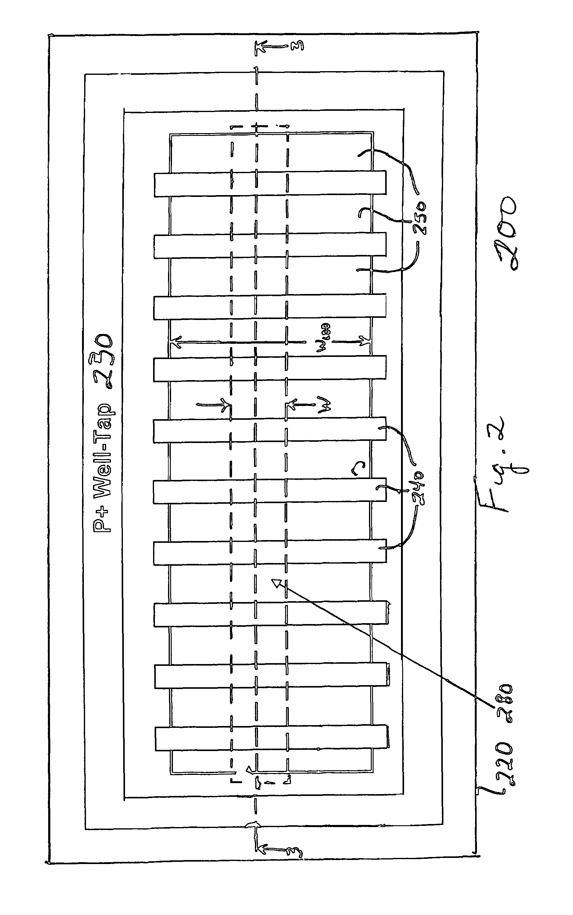
[0013]FIG. 2 is a top view of a preferred embodiment of an electrostatic discharge (ESD) protection device 200 of the present invention. Device 200 is formed in a portion of a semiconductor substrate 210. A P-well 220 is formed in that portion and electrical connection to the P-well is made through P+ well taps 230. Illustratively, the P-well tap extends around the entire periphery of P-well 220. An NMOS transistor is formed in the P-well having a plurality of gate fingers 240 and N+ source / drain regions 250 on both sides of the gate fingers. While not shown in FIG. 2, N-type lightly doped drain (LDD) regions extend toward each other from the source / drain regions 250 on both sides of each gate finger 240. In addition, underneath at least a portion of each N-type LDD region is a P-type region that forms a P-N junction with the drain / source region. In the embodiment of FIG. 2, the location of the P-type region and therefore the location of the P-N junction is indicated generally by th...


PUM


Abstract

An integrated circuit is disclosed comprising at least one I / O pull-down device for protecting I / O logic circuits from electrostatic discharge (ESD). The turn-on voltage of the parasitic bipolar transistor in the I / O pull-down device is lowered by forming under a portion of the lightly doped drain (LDD) region of a first conductivity type of a conventional MOS transistor a second region of a second conductivity type. A P-N junction is formed between the second region and the source / drain regions. The turn-on voltage of the parasitic bipolar transistor in the I / O pull-down device can be reduced by at least 3 volts from that of a comparable device that does not practice the invention and can be varied by varying the concentration of the dopant. A method for forming the circuit including a process for recovering the current of the I / O pull-down device and its advantages are also disclosed.

Description

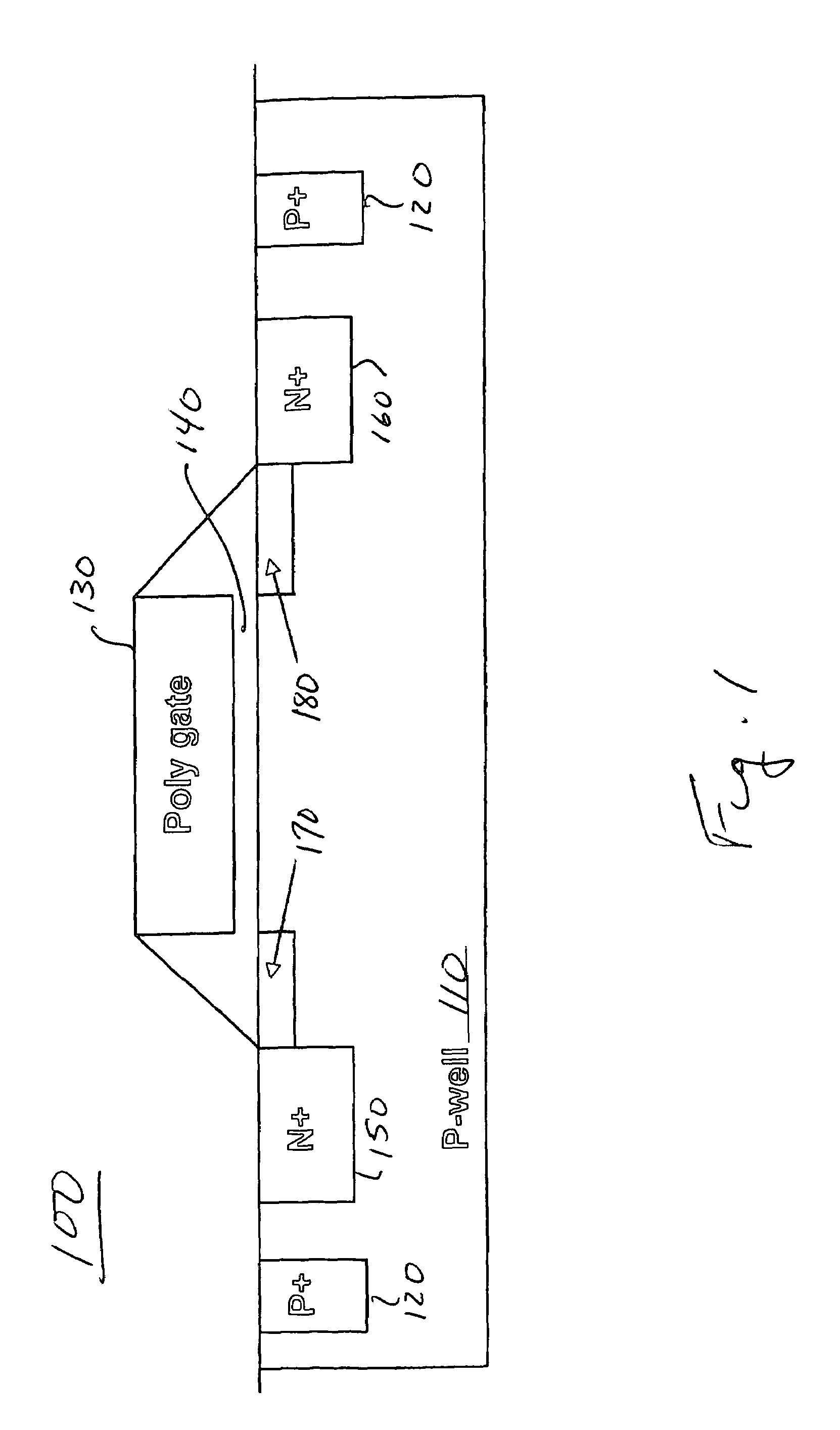
CROSS-REFERENCE TO RELATED APPLICATIONS[0001]This application is a continuation-in-part of application Ser. No. 10 / 882,874 filing date Jun. 30, 2004 which is a divisional of application Ser. No. 10 / 298,104, now U.S. Pat. No. 6,777,721, all of which are incorporated herein by reference.BACKGROUND OF THE INVENTION[0002]I / O pull-down devices have regularly been used to protect I / O logic circuits from electrostatic discharge (ESD). One such I / O pull-down device 100 is shown in FIG. 1. Device 100 comprises a P-well or P-type substrate 110 having P+ taps or contacts 120, a polysilicon gate 130 on the substrate and insulated therefrom by gate oxide 140, heavily doped N-type source and drain regions 150, 160, and N-type lightly doped drain (LDD) regions 170, 180 extending toward each other in the substrate from the source and drain regions. A parasitic NPN bipolar transistor is formed in this device in which the source and drain regions 150, 160 are the emitter and collector of the transist...

Claims


Application Information

Patent Timeline
IPC IPC(8): H01L23/62
CPCH01L27/0277H01L29/1083H01L29/6659
Inventor O, HUGH SUNGKISHIH, CHIH-CHINGHUANG, CHENG-HSIUNGLIU, YOW-JUANG BILL
Owner ALTERA CORP
Learn More