Semiconductor device with semiconductor layer having various thickness

a semiconductor device and semiconductor layer technology, applied in the direction of semiconductor devices, electrical devices, transistors, etc., can solve the problems of reducing the drain breakdown voltage, the impracticability of suppressing the “diffraction electric field” still remains, and the area penalty, so as to enhance the effect of the semiconductor device, suppress the parasitic bipolar effect, and reduce the thickness of the first impurity layer

Inactive Publication Date: 2008-04-15
TESSERA ADVANCED TECH
View PDF20 Cites 0 Cited by
  • Summary
  • Abstract
  • Description
  • Claims
  • Application Information

AI Technical Summary

Benefits of technology

[0032]In the semiconductor device of the fifth aspect, the presence of a metal compound layer allows lifetime killers to be formed in the semiconductor layer between the first impurity layer and the insulating layer.
[0033]In the semiconductor device of the sixth aspect, it is easy to bring the depletion layer in contact with the isolating layer while reducing the thickness of the first impurity layer.
[0034]The semiconductor devices of the seventh and eighth aspects can enhance the effect of the semiconductor device of the sixth aspect.
[0035]Unlike the structure in which the first impurity layer is in contact with the insulating layer, the semiconductor devices of the ninth and tenth aspects include distortion of the band structure over a wide range. This suppresses accumulation of carriers (holes for an NMOS) in the vicinity of the source and the parasitic bipolar effect.
[0036]In the semiconductor device of the eleventh aspect, lifetime killers such as crystal defects, crystal distortion, point defects, and recombination centers are produced at the interfaces and its vicinity between the insulating layer and each of the semiconductor layer and the first impurity layer. This suppresses the parasitic bipolar effect.
[0037]In view of the still remaining problems in the conventional first through third techniques, an object of the present invention is to provide an SOIMOS transistor having small junction capacitance even with low drain voltage and capable of suppressing the floating-body effect.

Problems solved by technology

This produces a kink effect of reducing a threshold voltage of the SOIMOS transistor and thereby causing a sudden local change in drain current in the vicinity of certain drain voltage (voltage applied between source and drain) and causes a problem of reducing a drain breakdown voltage.
In either of the first and second conventional techniques, however, the source 51 and the drain 52 reach the buried oxide film 2 through the SOI layer 4, so a problem of the impracticability of suppressing a “diffraction electric field” still remains.
This structure, however, requires a body terminal for drawing holes and the formation of a body terminal may cause an area penalty.
Further, effects achieved by the method for drawing holes through a body terminal vary according to the location of a body contact region; therefore, a problem of pattern dependence arises.

Method used


Image

  • Semiconductor device with semiconductor layer having various thickness
  • Semiconductor device with semiconductor layer having various thickness
  • Semiconductor device with semiconductor layer having various thickness

Examples


first preferred embodiment

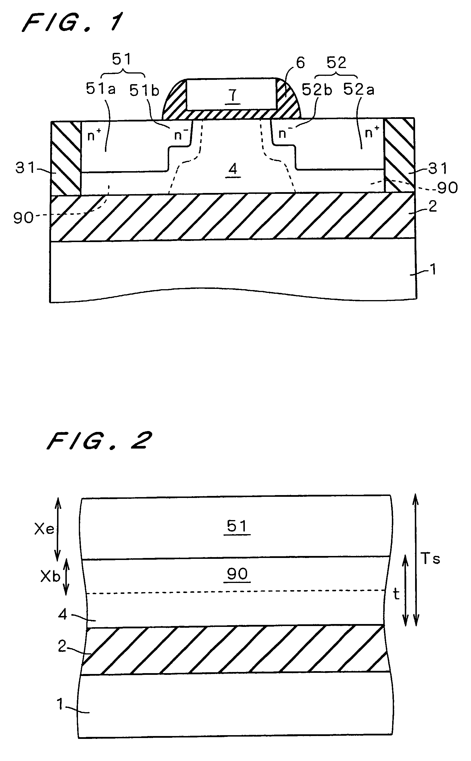
[0055]FIG. 1 is a cross-sectional view showing the structure of an SOIMOS transistor according to a first preferred embodiment of the present invention. On a buried oxide film 2 formed on a p-type semiconductor substrate 1 made for example of silicon, an SOI layer 4, which is to be a body along with a channel region, is formed and an n-type source 51 and an n-type drain 52 are formed in the surface of the SOI layer 4 on the opposite side of the buried oxide film 2. The bottoms of the respective source and drain 51, 52 are kept from contact with the buried oxide film 2. For example, the source 51 and the drain 52 have LDD (Lightly-doped Drain) structures; more specifically, the source 51 includes a region 51a with high impurity concentration and a region 51b with low impurity concentration, while the drain 52 includes a region 52a with high impurity concentration and a region 52b with low impurity concentration.

[0056]The SOI layer 4 sandwitched between the source 51 and the drain 52 ...

second preferred embodiment

[0067]By introducing lifetime killers to the structure of the first preferred embodiment the effect of the first conventional technique can further be enhanced. FIG. 5 is a cross-sectional view showing the structure of an SOIMOS transistor according to a second preferred embodiment. This structure is characteristically different from the structure of FIG. 1 in that lifetime killers 54 are introduced into the SOI layer 4 between the buried oxide film 2 and the source and drain 51, 52. In the second preferred embodiment, the relations between the equations (1) to (3) should preferably be maintained but it is not an absolute necessity.

[0068]When the thickness Ts of the SOI layer 4 is 1,000 Å, for example, the source 51 and the drain 52 are formed by implanting arsenic ions into the SOI layer 4 at an energy of 20 keV or less so that they are kept from contact with the buried oxide film 2. After the formation of the source 51 and the drain 52, argon ions are implanted at an angle of 30 d...

third preferred embodiment

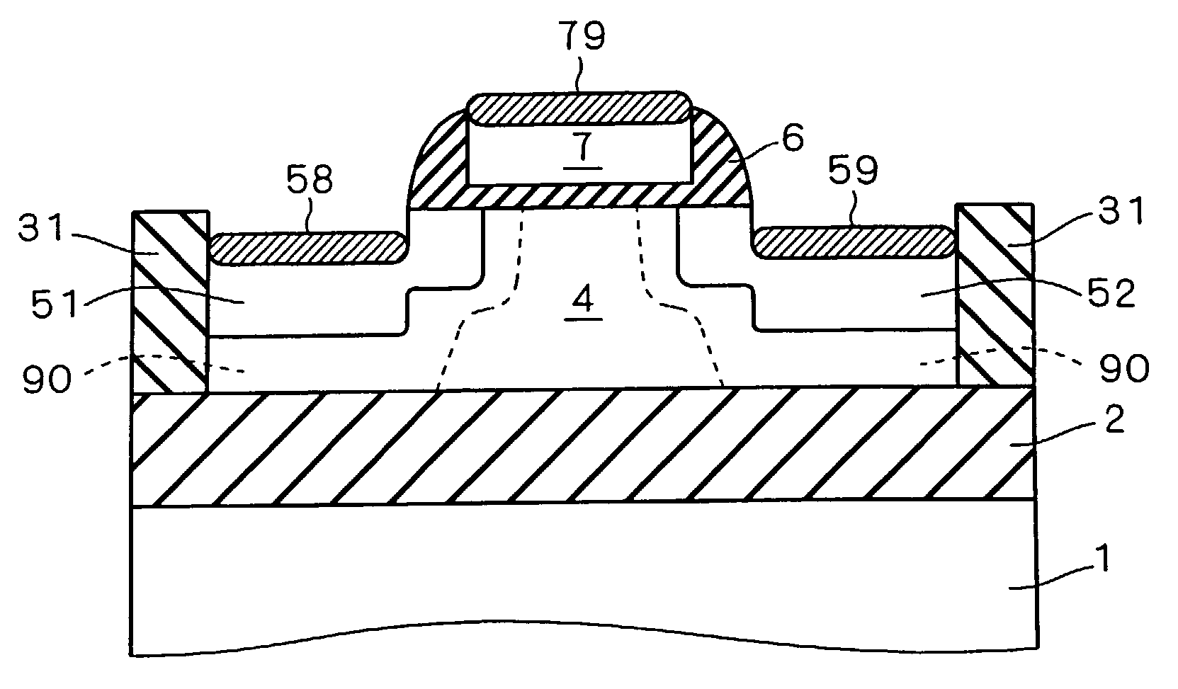
[0076]FIG. 6 is a cross-sectional view showing the structure of an SOIMOS transistor according to a third preferred embodiment of the present invention. This structure is characteristically different from that of FIG. 1 in that metal compound layers, e.g., silicide layers 58, 59, 79, are formed on the source 51, the drain 52, and the gate electrode 7, respectively. In the third preferred embodiment, the relations between the equations (1) to (3) should preferably be maintained but it is not an absolute necessity.

[0077]When the bottoms of the source 51 and the drain 52 are kept from contact with the buried oxide film 2 as in the first preferred embodiment, the formation of the silicide layers 58 and 79 produces lifetime killers as in the second preferred embodiment. That is, it is considered that crystal defects, crystal distortion, point defects, and recombination centers are produced by silicidation. Thus, the same effect as in the second preferred embodiment can be obtained. Areas...


PUM


Abstract

An SOI layer is provided in a buried oxide film and a source and a drain are provided on the upper surface of the SOI layer so that they are kept from contact with the buried oxide film. A depletion layer formed by the source, the drain, and the SOI layer extends to reach the buried oxide film, so parasitic capacitance is reduced. This structure achieves an SOIMOS transistor capable of reducing junction capacitance at low drain voltage.

Description

BACKGROUND OF THE INVENTION[0001]1. Field of the Invention[0002]The present invention relates to a silicon-on-insulator metal-oxide semiconductor transistor (hereinafter referred to as an SOIMOS transistor), more particularly relates to a technique for suppressing a floating-body effect in the transistor.[0003]2. Description of the Background Art[0004]Great attention is now focused on SOIMOS transistors as high-speed, low-power devices and their application to LSI for portable equipment for example is expected.[0005]A conventional SOIMOS transistor, however, has its body in a floating state, thus producing a parasitic bipolar effect that one type of carriers which are produced by impact ionization in the vicinity of the drain (e.g., holes for n-type SOIMOS transistors and electrons for p-type SOIMOS transistors) are accumulated in the vicinity of the source, whereby a parasitic bipolar transistor comprised of source, body, and drain enters into its active state. This produces a kink...

Claims


Application Information

Patent Timeline
Patent Type & Authority Patents(United States)
IPC IPC(8): H01L27/01H01L21/336H01L21/84H01L29/78H01L27/12H01L29/786
CPCH01L21/84H01L27/1203H01L29/66772H01L29/78612H01L29/78621H01L29/78
Inventor MATSUMOTO, TAKUJIMAEDA, SHIGENOBU
Owner TESSERA ADVANCED TECH
Why Eureka
Try Eureka