Stationary fourier transform spectrometer

a technology of transform spectrometer and spectrometer, which is applied in the direction of interferometric spectrometry, optical radiation measurement, instruments, etc., can solve the problems of complex adjustment of interferometer, high theoretical performance of spectrometer, and limited practical implementation

Active Publication Date: 2008-02-12
OFFICE NAT DETUD & DE RECH AEROSPATIALES
View PDF2 Cites 18 Cited by
  • Summary
  • Abstract
  • Description
  • Claims
  • Application Information

AI Technical Summary

Benefits of technology

[0020]Thanks to the variation in the thickness of the plate from one region to the other, and therefore of the phase difference parameter variation from one pixel to the other, a stationary Fourier transform spectrometer is obtained. The relative location on the detection plane of a region inducing a optical path difference δ with a region inducing a optical path difference δ+dδ or δ−dδ may take any value. The spectrometer of the invention is therefore very compact, since the image plane coincides both with the first face of the plate and the active faces of the photosensitive elements, and thus integrates against the detector a two-wave interferometer benefiting from both modern detector fabrication technologies and the intrinsic performance capabilities of stationary Fourier transform spectrometers.

Problems solved by technology

Such spectrometers offer high performance in theory, but are subject to practical implementation limitations, related in particular to the opto-mechanical adjustment of the interferometer.
The interferometer proves complicated to adjust, in particular in radiation bands where the monitoring means are not visual.
These practical constraints intrinsic to the spectrometer, added to the external constraints linked to experimental, on-board or field conditions, lead to the production of spectrometer prototypes that are costly, fragile and bulky.

Method used


Image

  • Stationary fourier transform spectrometer
  • Stationary fourier transform spectrometer
  • Stationary fourier transform spectrometer

Examples


Embodiment Construction

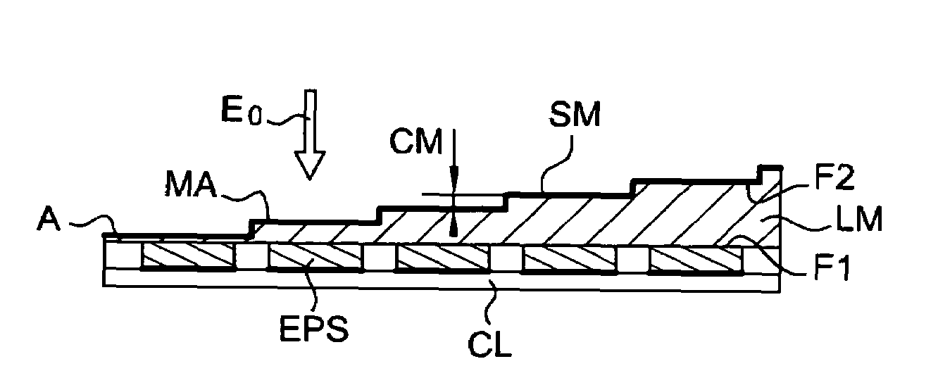
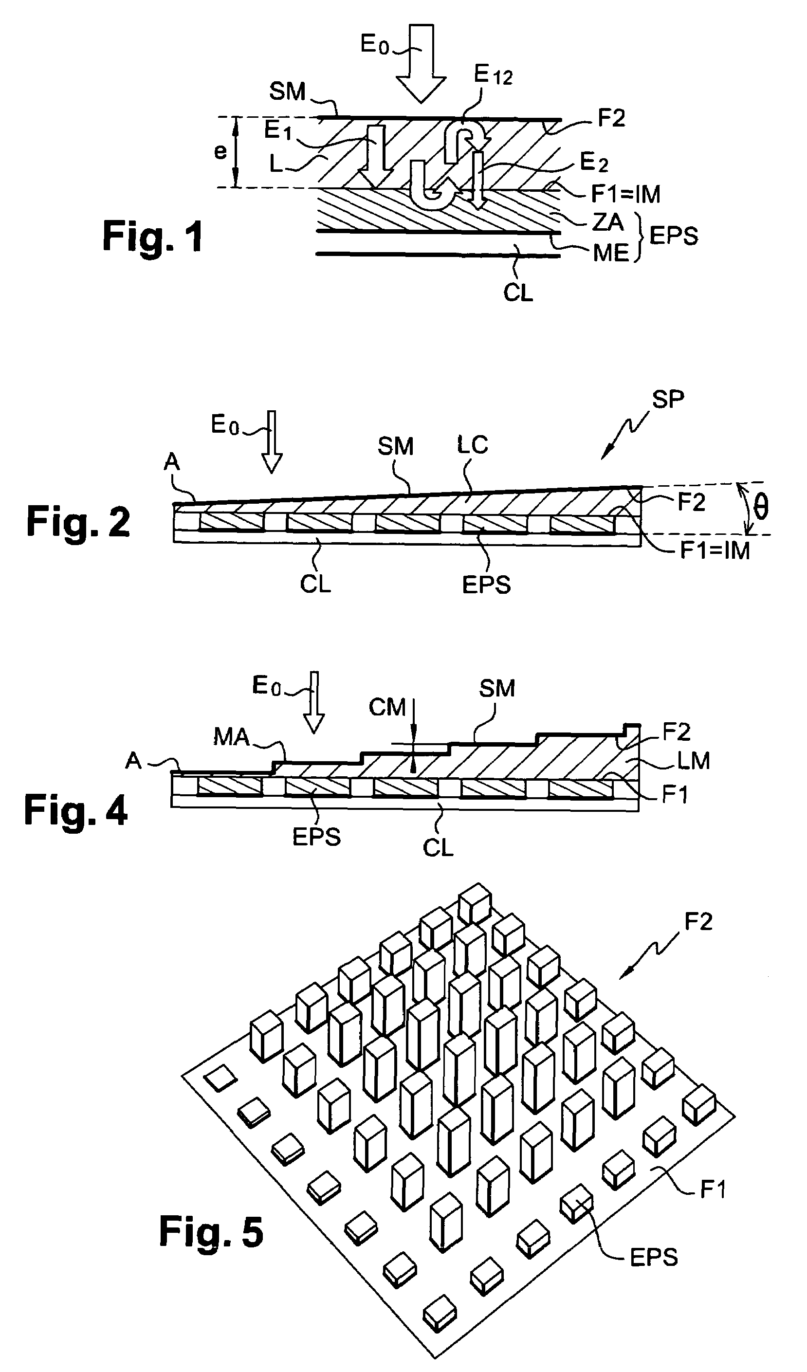
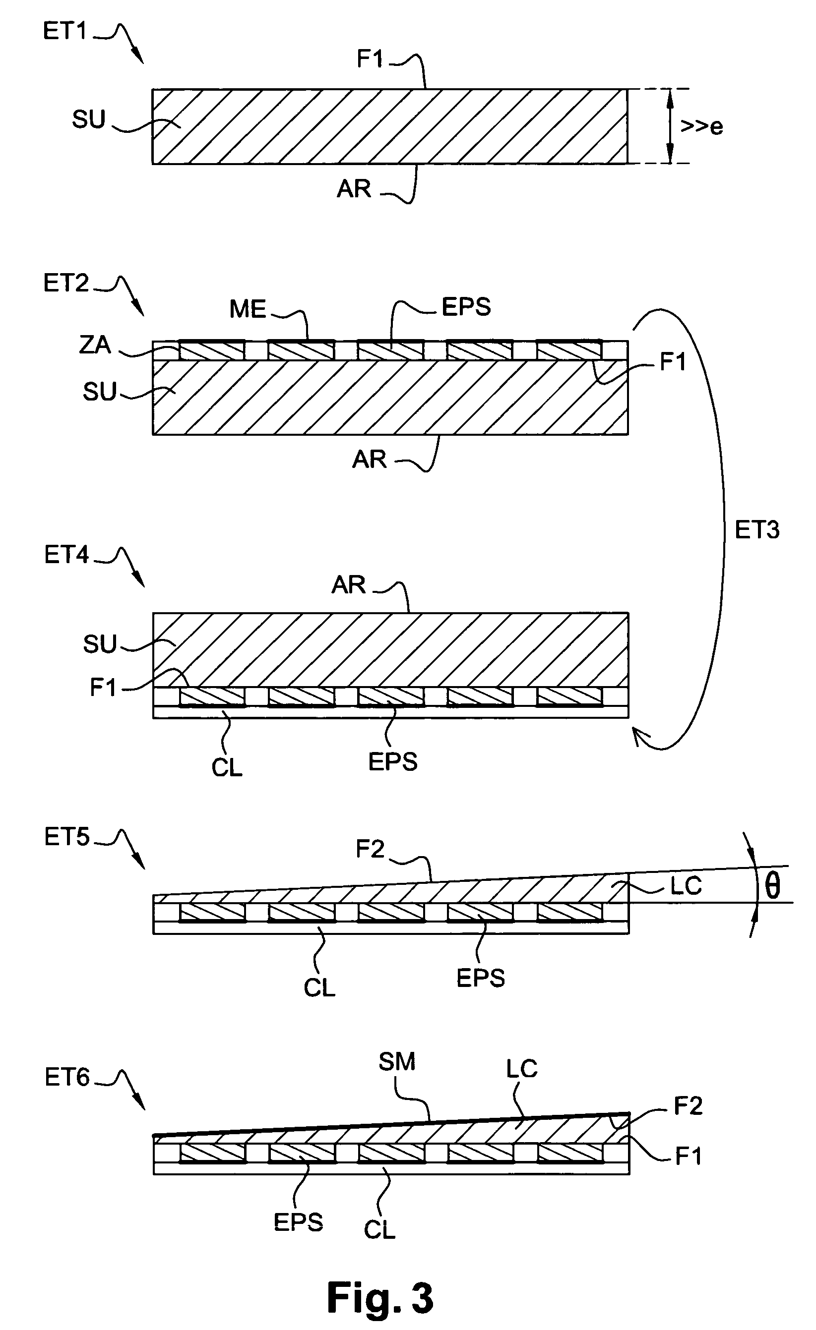
[0035]With reference to FIG. 1, a photosensitive element EPS with a semiconductor heterostructure in a detector is shown. The element EPS relates to a detected picture element, called a pixel. It has a sensitive face constituting an image plane IM over a photosensitive active region ZA that absorbs the greater part of an incident wave E1. The other face of the element EPS integrates a read circuit CL including electrode and separated by an insulative layer from the active region ZA. The active region ZA and the read circuit CL are combined using a hybridation technique.

[0036]A plate L made of a material substantially transparent to the incident radiation is superposed on the photosensitive element EPS. For example, the plate L is made from a crystalline compound including a semiconductor, for example a telluride compound such as cadmium and zinc telluride Cd Zn Te having a refractive index n=2.7. The thickness e of the plate is from a few micrometers to a few tens of micrometers. A ...


PUM


Abstract

The invention aims to integrate a two-wave stationary interferometer on a photodetector during fabrication in order to constitute a miniature stationary Fourier transform spectrometer. The interferometer essentially comprises a plate having a first plane face coinciding with an image plane on semiconductor photosensitive elements and a second face that is not parallel to the first face. The second face reflects a wave that has a phase difference relative to the incident wave interfering with it that is a function of the local thickness of the plate.

Description

CROSS-REFERENCE TO RELATED APPLICATION[0001]The application claims priority under 35 U.S.C. §119 based on French Application No. 0306548, filed May 28, 2003, the entire disclosure of which is hereby incorporated by reference.BACKGROUND OF THE INVENTION[0002]1. Field of the Invention[0003]The present invention relates to detecting and quantitatively analyzing the spectral content of a light wave. It concerns more particularly a stationary Fourier transform spectrometer including a photodetector with semiconductor elements responsive particularly to incident radiation and a two-wave stationary interferometer comprising a semi-reflecting diopter.[0004]2. Description of the Prior Art[0005]A Michelson interferometer comprising a wave splitter and two mirrors, for example, imposes an optical path difference between two majority waves by positioning one of the mirrors relative to the other in translation or rotation. The intensity of the wave resulting from the phase difference of the two ...

Claims


Application Information

Patent Timeline
Patent Type & Authority Patents(United States)
IPC IPC(8): G01B9/02G01J3/45G01J3/453
CPCG01J3/26G01J3/4531G01J3/4532H01L27/1446H01L31/02165G01J3/0259
Inventor GUERINEAU, NICOLASDESCHAMPS, JOELROMMELUERE, SYLVAIN
Owner OFFICE NAT DETUD & DE RECH AEROSPATIALES
Why Eureka
Try Eureka