Method of manufacturing multilayer wiring board

a manufacturing method and wiring technology, applied in the direction of metallic pattern materials, solid-state devices, thermoplastic polymer dielectrics, etc., can solve the problems of large reduction in the modulus of elasticity, distortion of the conducting material which forms the wiring circuit, and the tendency of the production facility to increase in size, so as to achieve finely detailed conductive wiring and high degree of precision. , the effect of high degr

Inactive Publication Date: 2008-02-26
SONY CORP +1
View PDF39 Cites 8 Cited by
  • Summary
  • Abstract
  • Description
  • Claims
  • Application Information

AI Technical Summary

Benefits of technology

[0018]The present invention aims to resolve the problems described above, with an object of providing a multilayer wiring board with a high degree of heat resistance, which is capable of low temperature fusion without the occurrence of resin flow, enables high precision, finely detailed conductive wiring, can be ideally applied to low volume high mix manufacturing configurations, and also has little impact on the environment, as well as providing a semiconductor device mounting board using such a multilayer wiring board, and a method of manufacturing such a multilayer wiring board.
[0019]As a result of intensive research, the inventors of the present invention realized that if a substrate formed from a thermoplastic resin could be combined with a wiring pattern formed from a conductive paste to produce a wiring board, then a high performance, environmentally friendly multilayer wiring board could be produced, and were hence able to complete the present invention.

Problems solved by technology

However, although conventional highly heat resistant thermoplastic resins offer advantages as highly heat resistant substrate materials, when the thermoplastic resin is laminated and integrated into a single unit, the resin must be heated to a temperature close to the resin melting point to ensure thermal fusion, and a problem arises during this heating and thermal fusion in that a resin flow, resulting from the large reduction in the modulus of elasticity at temperatures near the melting point, may cause distortions in the conducting material which forms the wiring circuit.
In addition, conventional printed wiring board production lines are suited to high volume low mix production, and consequently there is tendency for the production facilities to increase in size.
Furthermore, chemical etching (wet etching) and plating techniques are typically used during the formation of wiring circuits on the printed wiring boards, and these techniques are undesirable from the viewpoint of environmental impact.
Furthermore as described above, examples of methods for wiring formation using dry processes include screen printing methods and dispensing methods using a conductive paste, although in both of these methods, there is a limit to the improvements in detail and precision of the conductive wiring which can be achieved in order to try and meet the ever increasing demands for higher density mounting.
In addition, as described above, in a laminated product of a thermoplastic resin on which a wiring circuit has been formed using a conductive paste, the resin must be heated to a temperature close to the melting point and subjected to pressure to fuse the thermoplastic resin layers together to create a single integrated unit, and as the pitch of the wiring becomes finer, distortion of the wiring resulting from resin flow during lamination is increasingly becoming a factor which cannot be ignored in substrate design.

Method used


Image

  • Method of manufacturing multilayer wiring board
  • Method of manufacturing multilayer wiring board
  • Method of manufacturing multilayer wiring board

Examples


first embodiment

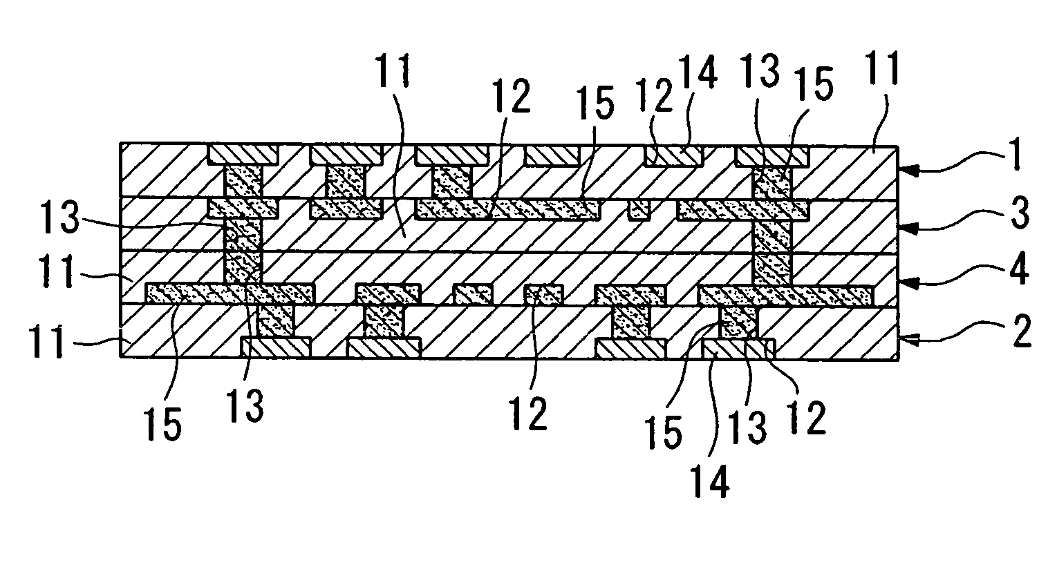
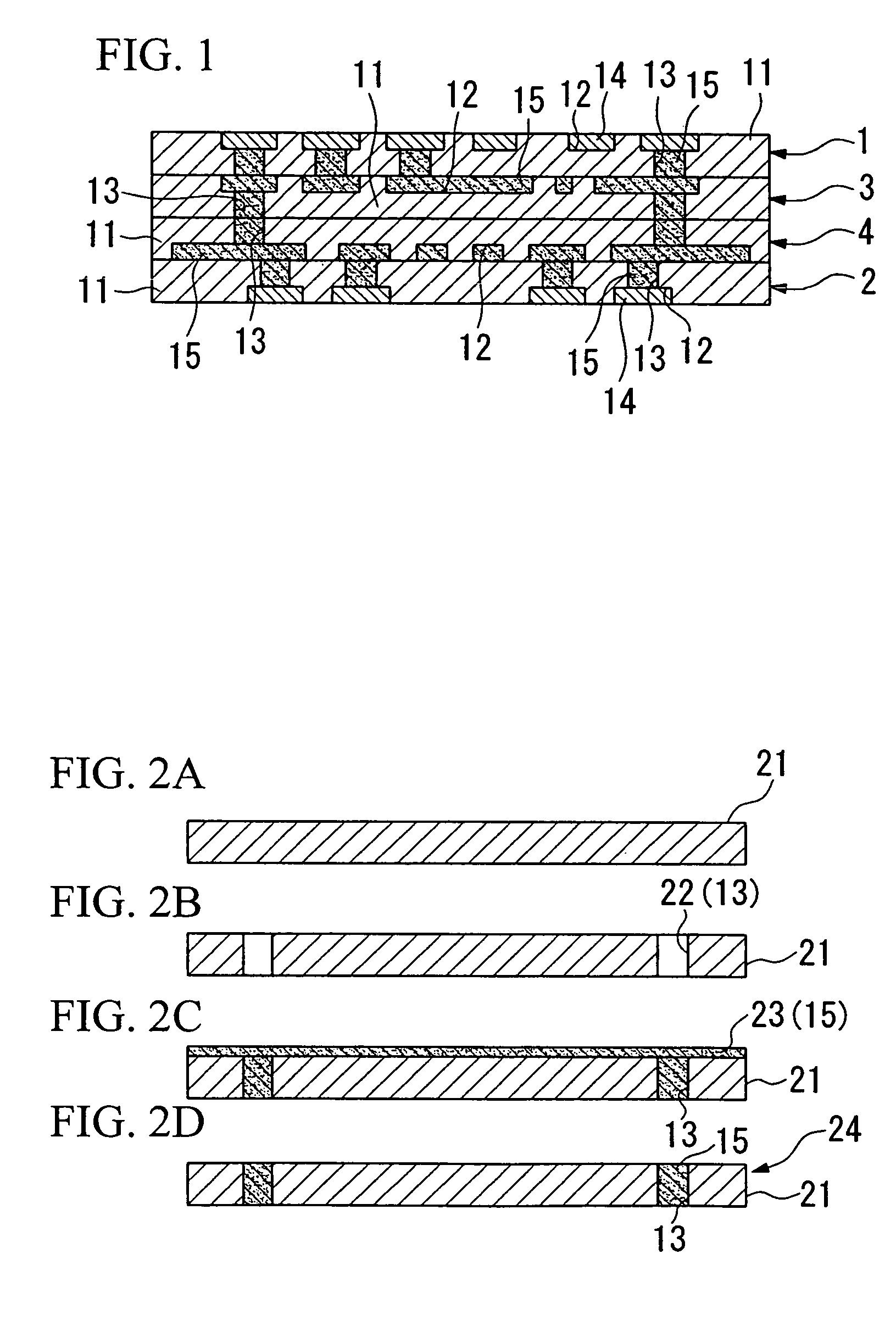
[0046]FIG. 1 is a cross-sectional diagram showing a multilayer wiring board according to a first embodiment of the present invention. In the figure, symbol 1 represents an uppermost layer substrate (a wiring substrate of the uppermost layer), symbol 2 represents a lowest layer substrate (a wiring substrate of the lowest layer), and symbols 3 and 4 represent inner layer substrates (wiring substrates) sandwiched between the uppermost layer substrate 1 and the lowest layer substrate 4.

[0047]The uppermost layer substrate 1 is typically a film, a thin plate or a sheet of a thickness of no more than 100 μm, wherein grooves 12 for forming a wiring circuit are formed in one surface (the upper surface in the figure) of an insulating substrate 11 formed from a film, a thin plate or a sheet of a thermoplastic resin composition comprising a polyarylketone resin with a crystalline melting peak temperature of at least 260° C. and an amorphous polyetherimide resin as the primary constituents, via ...

second embodiment

[0096]FIG. 7 is a cross-sectional diagram showing an IC package board (a semiconductor device mounting board) of a second embodiment of the present invention.

[0097]This IC package board is a multilayer interposer board 61 comprising a lowest layer substrate 35, an inner layer substrate 49 and an inner layer substrate 50 laminated together in this sequence and integrated into a single unit by thermal fusion, and an IC chip (semiconductor device) 63 is fixed directly to the top of the inner layer substrate 50 which functions as an IC chip (semiconductor device) mounting section, so that the pins (terminals) 64 of the IC chip 63 and the conductive circuit 46 are electrically connected, and the IC chip 63 is then sealed with a sealing resin 65 such as an epoxy resin.

[0098]In order to manufacture this IC package board, first, as shown in FIG. 8A, a cushion film 52 with good elasticity and releasability, a lowest layer substrate 35, an inner layer substrate 49, an inner layer substrate 50...

third embodiment

[0104]FIG. 9 is a cross-sectional diagram showing an IC package board (a semiconductor device mounting board) of a third embodiment of the present invention.

[0105]This IC package board differs from the IC package board of the second embodiment in that whereas in the IC package board of the second embodiment, the IC chip 63 was fixed directly onto the inner layer substrate 50 which functions as the IC chip mounting section, in the IC package board of this embodiment, the IC chip 63 is fixed to the top of the inner layer substrate 50, which functions as the IC chip mounting section, via an IC chip fixing adhesive 62.

[0106]In order to manufacture this IC package board, a multilayer interposer board 61 is first prepared in the same manner as described for the IC package board of the second embodiment, and then, as shown in FIG. 10A, the IC chip fixing adhesive 62 is applied to the top of the inner layer substrate 50 which functions as the IC chip mounting section, an IC chip 63 is mount...


PUM

PropertyMeasurementUnit
glass transition temperatureaaaaaaaaaa
melting peak temperatureaaaaaaaaaa
crystalline melting peak temperatureaaaaaaaaaa

Abstract

A method of manufacturing a, in order to accommodate the words range and to clarify the multilayer wiring board, grooves for forming a wiring circuit and via holes are formed in an insulating substrate formed from a thermoplastic resin composition comprising a polyarylketone resin with a crystalline melting peak temperature of at least 260° C. and an amorphous polyetherimide resin as the primary constituents, a metallic foil is embedded within the grooves so that the surface of the foil protrudes to the surface of the insulating substrate, and a conductive material formed by curing a conductive paste is used for filling the via holes.

Description

CROSS-REFERENCE TO RELATED APPLICATIONS[0001]This application is a divisional of U.S. patent application Ser. No. 10 / 357,183, filed Feb. 3, 2003 now U.S. Pat. No. 6,797,367, which is hereby incorporated by reference in its entirety.BACKGROUND OF THE INVENTION[0002]1. Field of the Invention[0003]The present invention relates to a multilayer wiring board, a semiconductor device mounting board using such a wiring board, and a method of manufacturing such a multilayer wiring board.[0004]2. Description of the Background Art[0005]In recent years, the trend towards increased miniaturization and functionality of electronic equipment has produced a growing demand for higher density mounting of electronic components on the mounting boards used for mounting such electronic equipment. In order to enable these electronic components to be mounted on the mounting boards with higher densities, there are calls not only for further miniaturization of the electronic components, but also for finer and ...

Claims


Application Information

Patent Timeline
Patent Type & Authority Patents(United States)
IPC IPC(8): H01K3/22C08J5/18C08L71/10C08L79/08H01L23/12H01L23/14H05K1/03H05K1/09H05K3/04H05K3/10H05K3/20H05K3/22H05K3/40H05K3/46
CPCH05K1/0353H05K3/041H05K3/1258H05K3/4617H05K3/4632H01L2224/16Y10T29/49171H01L2924/0102H01L2924/01046H01L2924/01078H01L2924/09701H05K1/0373H05K1/095H05K3/045H05K3/107H05K3/4069H05K2201/0129H05K2201/0154H05K2201/0209H05K2201/0352H05K2201/0391H05K2203/0108H05K2203/065H01L2924/01019Y10S428/901Y10T29/49117Y10T29/49158Y10T29/49155Y10T29/49124Y10T29/49172Y10T428/24917H01L2224/83192Y10T428/249994Y02P20/582H05K1/05
Inventor OGAWA, MINORUIZUMI, MASAHIROITOH, SHIGEYASUYAMADA, SHINGETSUSUZUKI, SHUUJIKUROSAKI, HIROO
Owner SONY CORP
Why Eureka
Try Eureka