Method for making an integrated circuit substrate having embedded passive components

a technology of integrated circuit substrate and passive components, which is applied in the direction of resistor housing/enclose/embedding, conductive pattern formation, electrical apparatus construction details, etc., can solve the problems of not being able not being able to choose to integrate the passive components within the die, and mounting the passive components entails not only an added component cost, but the volume of the passive component package is consumed, so as to achieve low incremental cost

Inactive Publication Date: 2008-02-26
AMKOR TECH SINGAPORE HLDG PTE LTD
View PDF121 Cites 64 Cited by
  • Summary
  • Abstract
  • Description
  • Claims
  • Application Information

AI Technical Summary

Benefits of technology

[0007]A substrate having embedded passive components and methods for manufacturing provide a comp...

Problems solved by technology

Depending on the size of and power dissipation within the integrated circuit, and also the integrated circuit fabrication technology, it may not be possible to integrate the passive components within the die.
Further, for design of die for use with a variable range of passive components (e.g., passive components that set variable frequency characterist...

Method used


Image

  • Method for making an integrated circuit substrate having embedded passive components
  • Method for making an integrated circuit substrate having embedded passive components
  • Method for making an integrated circuit substrate having embedded passive components

Examples


Embodiment Construction

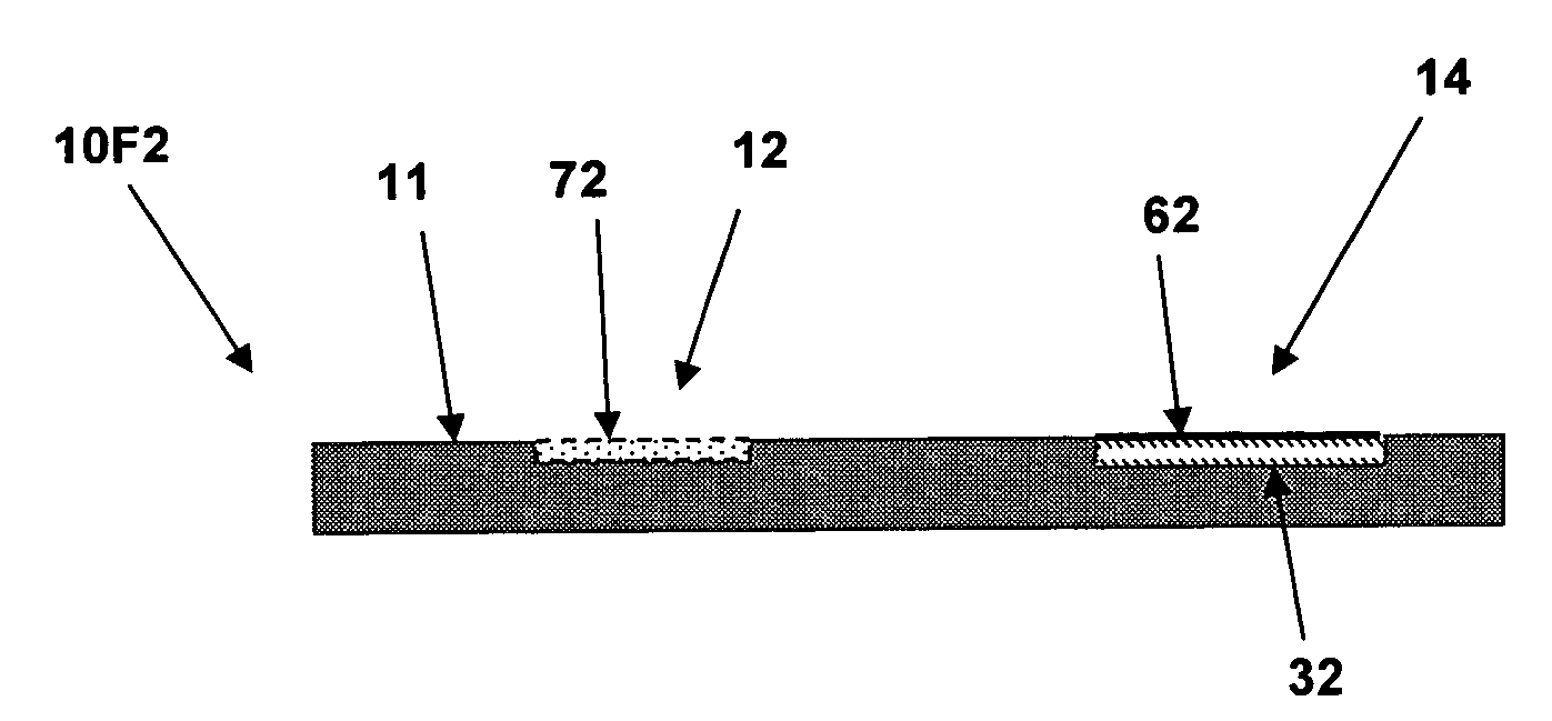
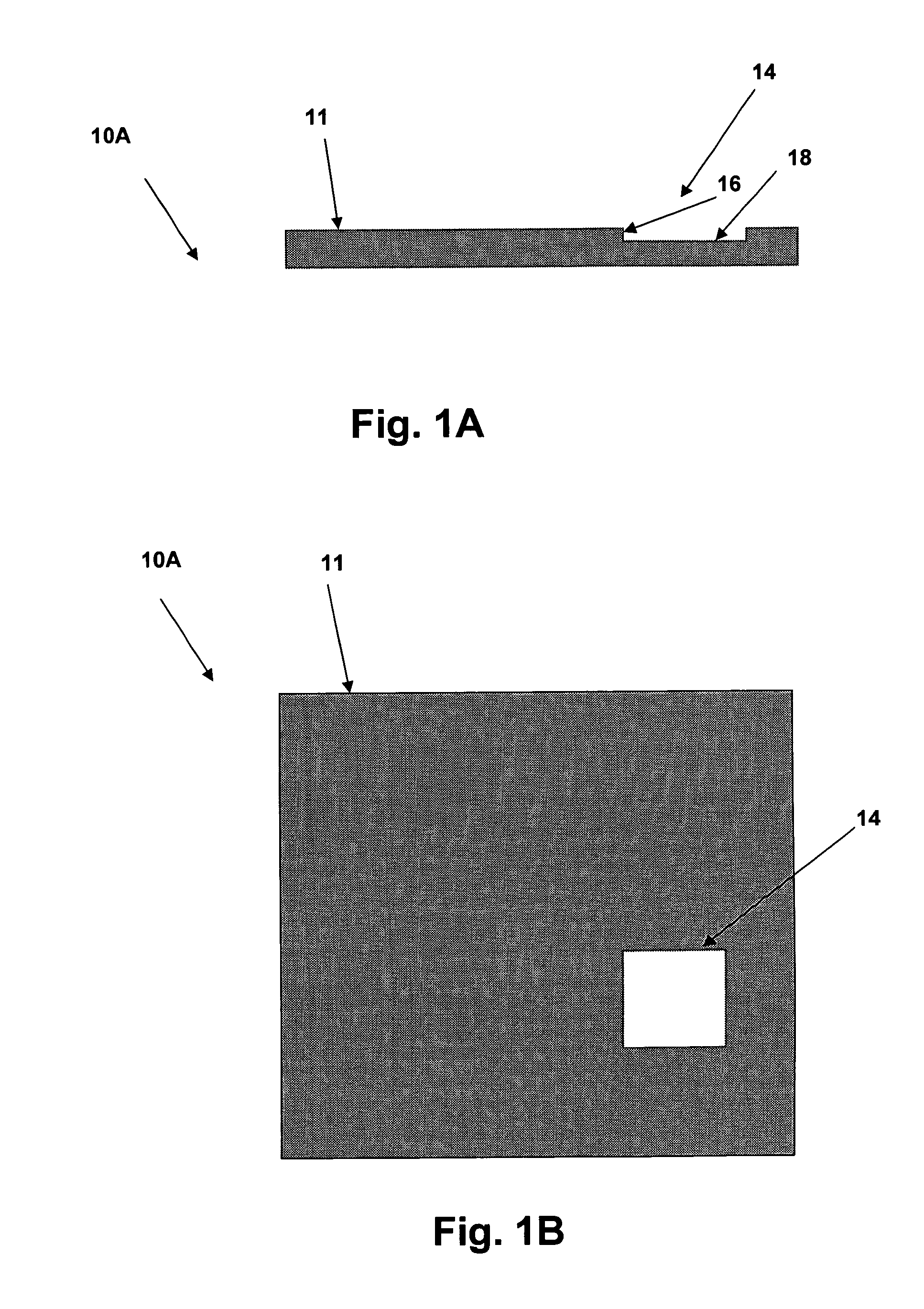
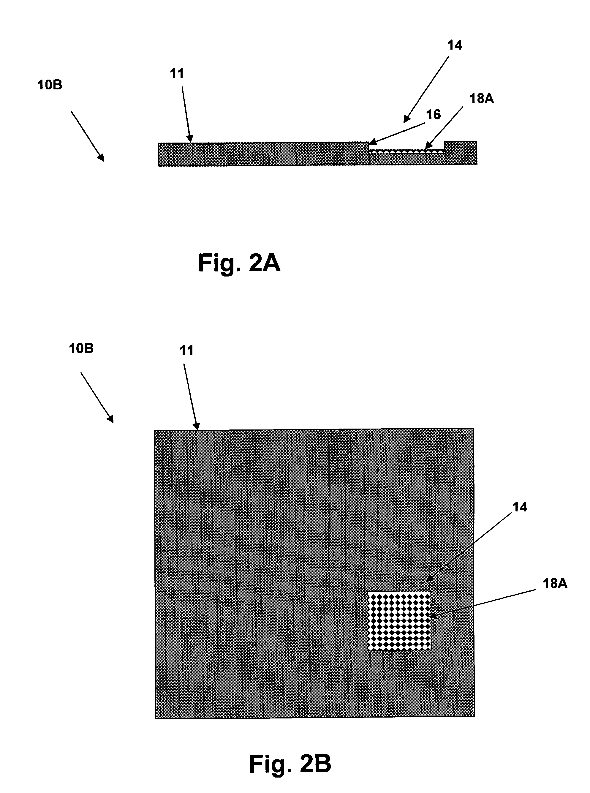
[0025]The above-incorporated patent applications disclose processes and structures for manufacturing a low-cost integrated circuit substrate having embedded circuit conductors. The present invention provides processes and structures for embedding and connecting passive components within such substrates, providing substrates with greatly expanded functionality at a lower cost than alternative circuits incorporating discrete passive components. The density of circuits is further improved using the techniques of the present invention and yield a higher density circuit integration than traditional discrete passive component techniques, as not only are the passive components moved inside of the semiconductor package, but typical interconnect and packaging areas and volumes associated with discrete passive components are eliminated. Packaging of passive components in the present invention is provided by the substrate within the semiconductor package, and the passive component interconnect...


PUM

PropertyMeasurementUnit
Dielectric polarization enthalpyaaaaaaaaaa
Electrical conductoraaaaaaaaaa
Surface areaaaaaaaaaaa

Abstract

A method for making an integrated circuit substrate having embedded passive components provides a reduced cost and compact package for a die and one or more passive components. An insulating layer of the substrate is embossed or laser-ablated to generate apertures for insertion of a paste forming the body of the passive component. A resistive paste is used to form resistors and a dielectric paste is used for forming capacitors. A capacitor plate may be deposited at a bottom of the aperture by using a doped substrate material and activating only the bottom wall of the aperture, enabling plating of the bottom wall without depositing conductive material on the side walls of the aperture. Vias may be formed to the bottom plate by using a disjoint structure and conductive paste technology. Connection to the passive components may be made by conductive paste-filled channels forming conductive patterns on the substrate.

Description

CROSS-REFERENCE TO RELATED APPLICATIONS[0001]The present application is a divisional of U.S. patent application Ser. No. 10 / 319,022 entitled “INTEGRATED CIRCUIT SUBSTRATE HAVING EMBEDDED PASSIVE COMPONENTS AND METHODS THEREFOR” filed on Dec. 12, 2002, now U.S. Pat. No. 6,987,661, issued Jan. 17, 2006, which is a Continuation-in-Part of U.S. patent application entitled “INTEGRATED CIRCUIT SUBSTRATE HAVING LASER-EMBEDDED CONDUCTIVE PATTERNS AND METHOD THEREFOR”, Ser. No. 10 / 138,225 filed May 1, 2002, now U.S. Pat. No. 6,930,256, issued Aug. 16, 2005, and having at least one common inventor and assigned to the same assignee. The Parent continuation-in-part application is also a continuation-in-part of U.S. patent application entitled “IMPRINTED INTEGRATED CIRCUIT SUBSTRATE AND METHOD FOR IMPRINTING AN INTEGRATED CIRCUIT SUBSTRATE”, Ser. No. 09 / 884,193 filed Jun. 19, 2001, now U.S. Pat. No. 6,967,124, issued Nov. 22, 2005, by the same inventors and assigned to the same assignee. The spe...

Claims


Application Information

Patent Timeline
IPC IPC(8): H01K3/10
CPCH05K1/167H05K1/162H05K1/0373Y10T29/49126H05K3/0032H05K3/107H05K3/1258H05K3/185H05K3/4069H05K2201/0187H05K2201/0236H05K2201/0347H05K2201/09036H05K2203/107Y10T29/49165Y10T29/49082Y10T29/49155Y10T29/417H01L2224/48091H01L2224/73265H01L2924/00014
Inventor HUEMOELLER, RONALD PATRICKRUSLI, SUKITANO
Owner AMKOR TECH SINGAPORE HLDG PTE LTD
Why Eureka
Try Eureka