
Method for image sensor protection

Inactive Publication Date: 2008-02-26
ADVANCED CHIP ENG TECH
View PDF4 Cites 11 Cited by
  • Summary
  • Abstract
  • Description
  • Claims
  • Application Information

AI Technical Summary

Benefits of technology

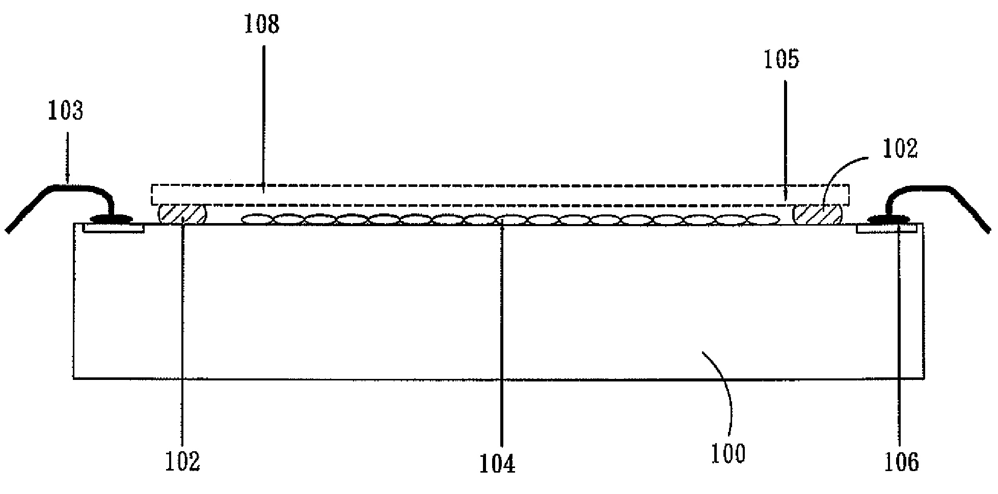
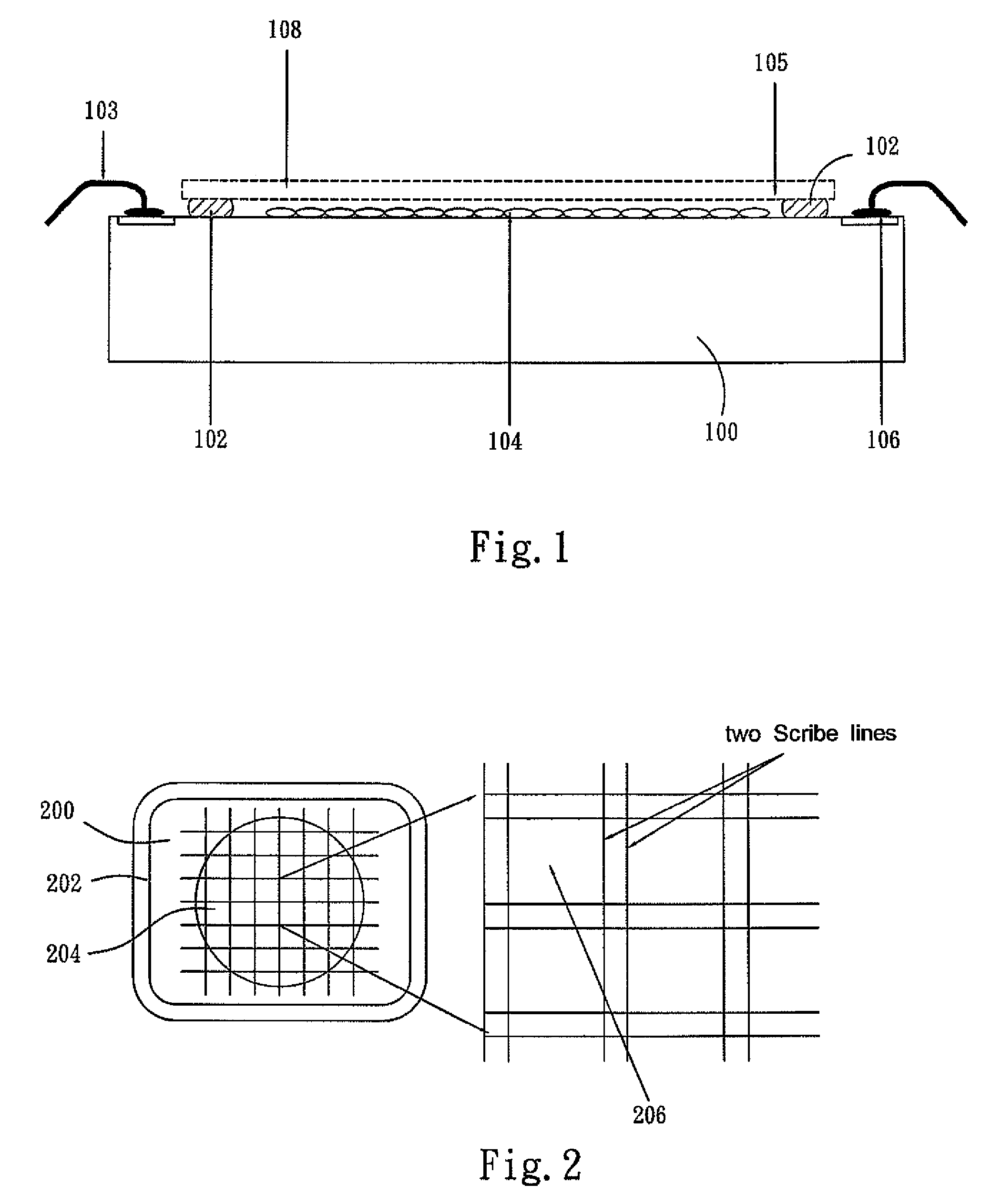
[0008]Therefore, the main objective of the present invention is to provide a protection method for image sensor, such as COB (Chip On Board) or FBGA (Fine-pitch Ball Grid Array) package structure, to prevent the sensor from particle contamination on micro lens.

Problems solved by technology

If the unwanted particles are not removed from the sensor, it leads to downgrade the quality of the device.
In order to achieve the purpose, the removal by manual may damage the sensitive chip.
One drawback of the COB is lower yield rate during packaging process due to particle contamination on sensing area.
Besides, the drawbacks of the LCC are higher packaging cost and lower yield rate due to particle contamination on sensing area.

Method used


Image

  • Method for image sensor protection
  • Method for image sensor protection
  • Method for image sensor protection

Examples


Embodiment Construction

[0016]Some sample embodiments of the invention will now be described in greater detail. Nevertheless, it should be recognized that the present invention can be practiced in a wide range of other embodiments besides those explicitly described, and the scope of the present invention is expressly not limited except as specified in the accompanying claims. Then, the components of the different elements are not shown to scale. Some dimensions of the related components are exaggerated and meaningless portions are not drawn to provide clearer description and comprehension of the present invention. The structure is adaptable to the FBGA (Fine-pitch Ball Grid Array) and COB (Chip On Board) type package. The present invention benefits lower cost and more simple process than the die scale package (CSP). The CSP type package suffers higher cost issue. Further, data processing speed of the FBGA package is far faster than conventional TSOP (Thin Small Outline Package) for inter-connection wires d...


PUM


Abstract

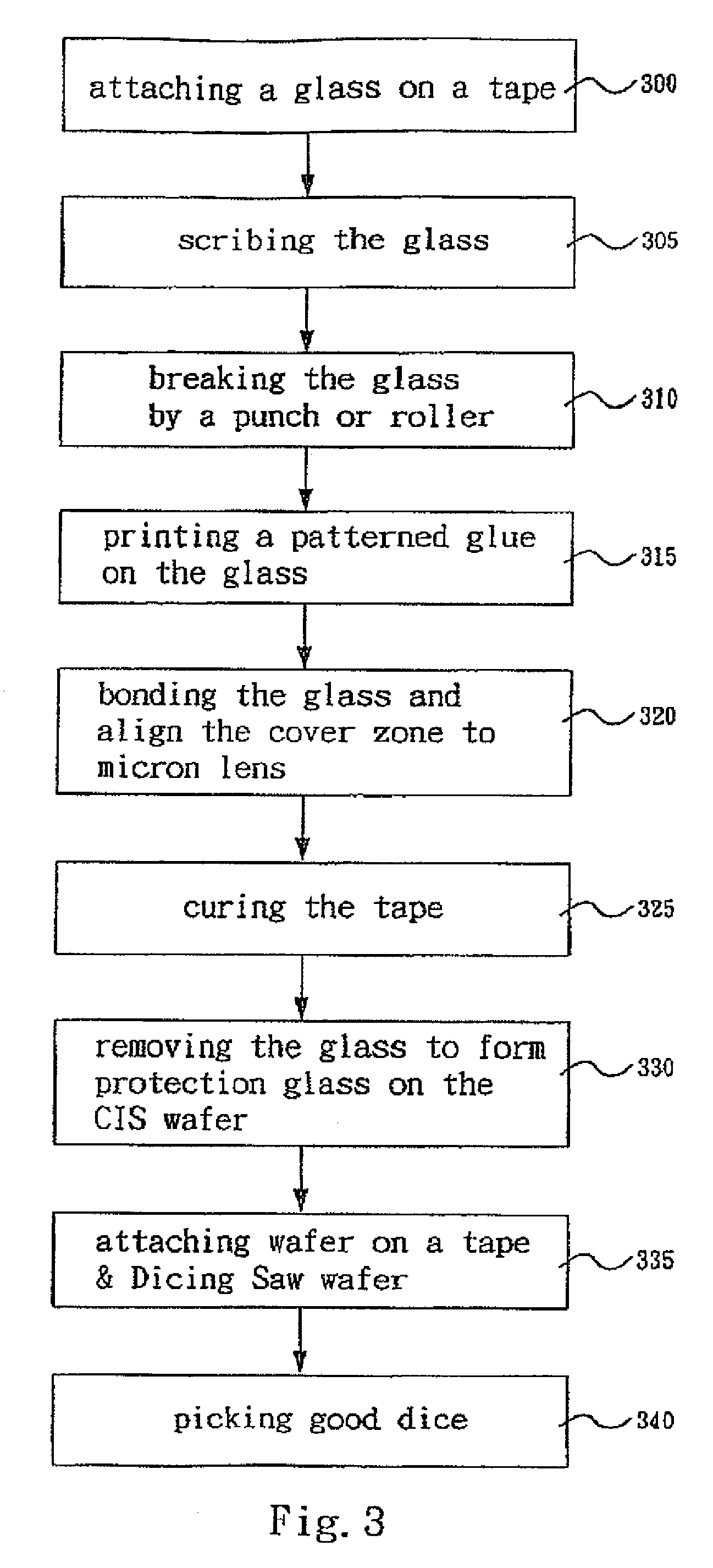
The method of forming image sensor protection comprises attaching a glass on a tape and scribing the glass with lines to define cover zones on the glass, the glass is then break by a rubber puncher followed by forming glue on the edge of the cover zones. The glass is bonded on a wafer with an image sensor to align the cover zones to a micron lens area of the image sensor, and then the tape is removed from the wafer, thereby forming glass with cover zones on the image sensor.

Description

FIELD OF THE INVENTION[0001]This invention relates to a CMOS image sensor (CIS), and more particularly to a protection method for the manufacture of an image sensor.BACKGROUND OF THE INVENTIONDescription of the Prior Art[0002]Most digital cameras include an image sensor or a photosensitive device, such as Complementary Metal-Oxide Semiconductor (CMOS) device to sense a scene. The photosensitive device reacts to light reflected from the scene the strength of that reaction into electronic charging signals. The camera can determine the specific color of each segment of the picture. Because the image is actually a collection of numeric data, it can easily be manipulated for more other effects. A digital image technique has been wildly applied to image shooting instrument such as digital camera, image scanner, etc. The conventional CMOS sensor is disposed on a circuit board. The CMOS sensor has a die secured therein. The lens seat has a focusing lens for focusing the image onto the die o...

Claims


Application Information

Patent Timeline
IPC IPC(8): H01L21/00H01L27/00
CPCH01L27/14618H01L27/14683H01L27/14643H01L27/148H01L2224/48463H01L2924/16235
Inventor YANG, WEN-KUNCHANG, JUI-HSIENHSU, HSIEN-WEN
Owner ADVANCED CHIP ENG TECH
Learn More