

Integrated circuit device, and method of fabricating same
a technology of integrated circuits and memory cells, which is applied in the direction of semiconductor devices, electrical equipment, transistors, etc., can solve the problems of difficult fabrication of integrated devices having soi logic transistors and soi memory cells
- Summary
- Abstract
- Description
- Claims
- Application Information
AI Technical Summary
Benefits of technology
Problems solved by technology
Method used
Image

Examples
Embodiment Construction
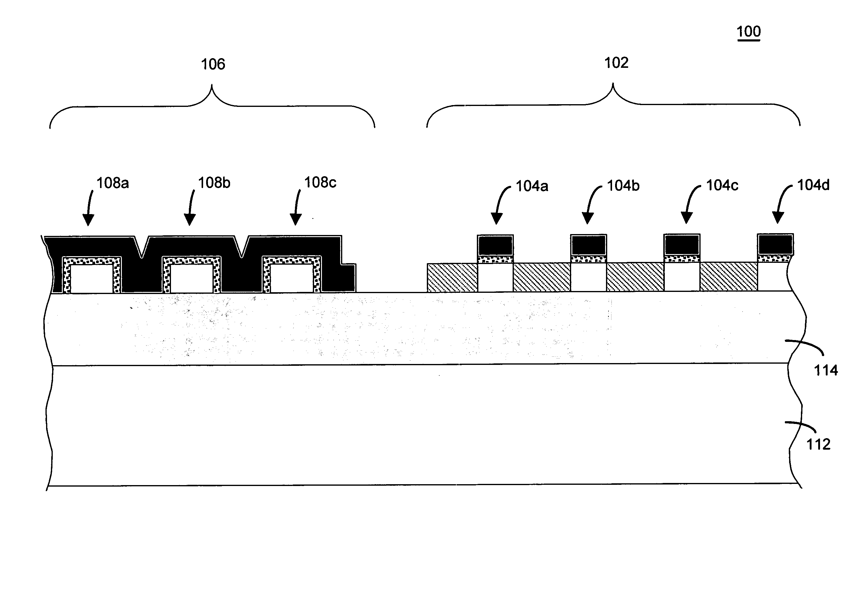
[0042]There are many inventions described and illustrated herein as well as many aspects and embodiments of those inventions. In a first aspect, the present invention is directed to integrated circuit device including SOI logic transistors and SOI memory transistors, and method for fabricating such a device. With reference to FIG. 5, in one embodiment, integrated circuit device 100 includes memory section 102 having, for example, PD or FD SOI memory cells 104a-d, and logic section 106 having, for example, high performance transistors 108a-c, such as Fin-FET, multiple gate transistors, and / or non-high performance transistors (for example, single gate transistors that do not possess the performance characteristics of high performance transistors—not illustrated).
[0043]With reference to FIG. 6, an exemplary method of fabricating or manufacturing an integrated circuit 100 according to one aspect of the present invention may begin with SOI wafer 110 including substrate 112 (comprised of,...
PUM
 Abstract
Description
Claims
Application Information