Application of different isolation schemes for logic and embedded memory

a technology of embedded memory and isolation scheme, which is applied in the direction of semiconductor devices, basic electric elements, electrical appliances, etc., can solve the problems of reducing the size of the die or component, reducing the size of the component, and reducing the size of the die, so as to facilitate semiconductor device fabrication, improve the isolation performance of the embedded memory portion, and increase the concentration of dopan

Active Publication Date: 2005-07-07
TEXAS INSTR INC
View PDF20 Cites 34 Cited by
  • Summary
  • Abstract
  • Description
  • Claims
  • Application Information

AI Technical Summary

Benefits of technology

[0007] The present invention facilitates semiconductor device fabrication by providing mechanisms for utilizing different isolation schemes within embedded memory and other logic portions of a device. The isolation performance of the embedded memory portion is improved relative to other portions of the device by increasing dopant concentration within well regions therein. As a result, smaller (n+-p+) isolation spacing can be employed thereby permitting a more compact design. The isolation in the logic portion uses lower doping / concentration than that of the embedded memory portion, which permits lower capacitance and therefore greater operational speed within the logic. Thus, reduced spacing is achieved within the memory portion without negatively impacting device performance within the logic portions of the die.

Problems solved by technology

One problem with utilizing individual components packaged separately is that great / substantial reductions in die or component sizes do not always yield the same reduction in component size due to the fact that packaging and interconnects do not generally reduce in proportion.
Thus, desired scaling / shrinking, which is a continuing demand for electronic devices, may not be obtained despite reduction in die sizes.
However, some desired space savings can be lost by combining multiple components onto a single die.
Fabrication procedures employed for multiple components may not be as well suited as procedures employed for single, specific components.

Method used


Image

  • Application of different isolation schemes for logic and embedded memory
  • Application of different isolation schemes for logic and embedded memory
  • Application of different isolation schemes for logic and embedded memory

Examples


Embodiment Construction

[0042] The present invention will now be described with respect to the accompanying drawings in which like numbered elements represent like parts. The figures provided herewith and the accompanying description of the figures are merely provided for illustrative purposes. One of ordinary skill in the art should realize, based on the instant description, other implementations and methods for fabricating the devices and structures illustrated in the figures and in the following description.

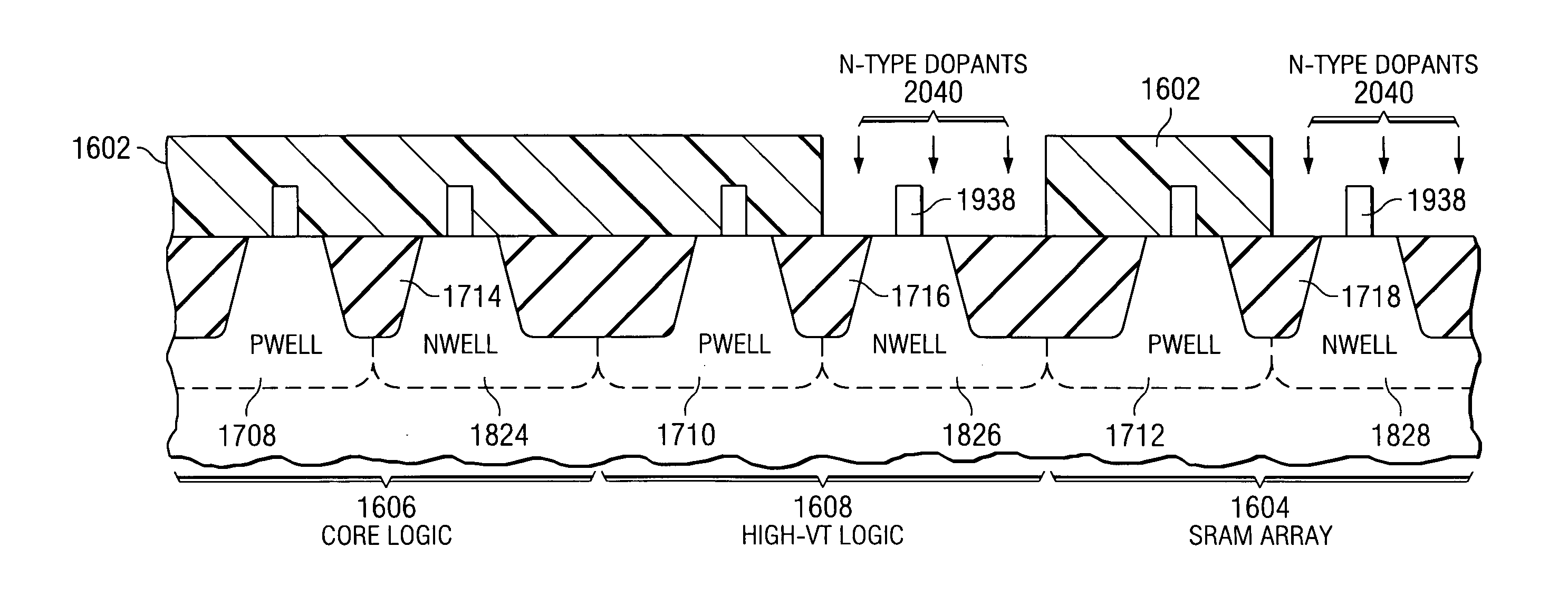
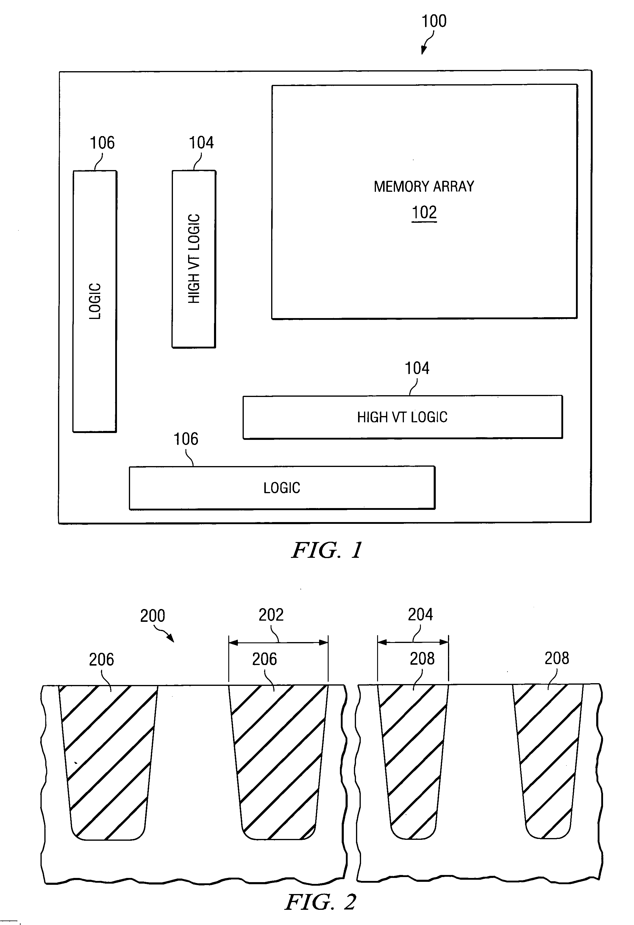
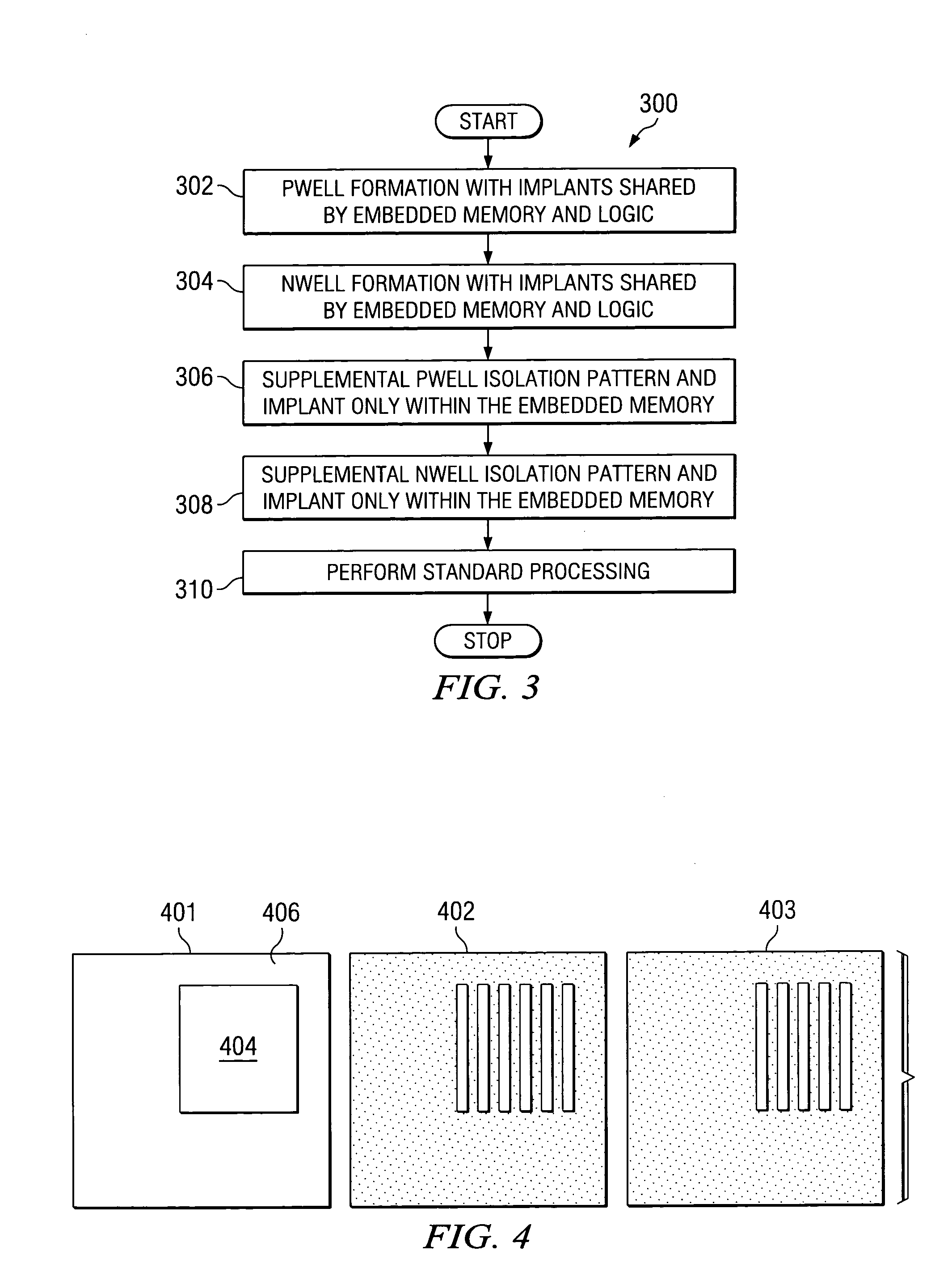
[0043] The present invention provides systems and methods that can reduce dimensions and area consumption of semiconductor devices by facilitating tighter spacing for an embedded memory portion of a semiconductor device. In conventional devices that include embedded memory, the same isolation doping profiles are employed for the embedded memory and logic portions of the device, limiting the extent to which memory n+-p+ isolation spacings (across well boundaries) can be reduced. However, the inventor...


PUM


Abstract

The present invention facilitates semiconductor device fabrication by providing mechanisms for utilizing different isolation schemes within embedded memory and other logic portions of a device. The isolation mechanism of the embedded memory portion is improved relative to other portions of the device by increasing dopant concentrations or reducing the depth of the dopant profiles within well regions of the embedded memory array. As a result, smaller isolation spacing can be employed thereby permitting a more compact array. The isolation mechanism of the logic portion is relatively less than that of the embedded memory portion, which permits greater operational speed for the logic.

Description

FIELD OF THE INVENTION [0001] The present invention relates generally to the field of semiconductor devices, and more particularly, to different isolation schemes for logic and embedded memory in semiconductor devices. BACKGROUND OF THE INVENTION [0002] Electronic devices typically include a number of individual components such as memory, logic, and the like. In the past, these individual components have been formed on separate die or chips. These separate chips were packaged separately and attached to one or more circuit boards of the electronic device. The circuit board contained the necessary interconnects to attain desired functionality from the individual components. As a result, the electronic device as a whole operated according to the individual components formed and interconnected via one or more circuit boards and electronic connections. [0003] One problem with utilizing individual components packaged separately is that great / substantial reductions in die or component size...

Claims


Application Information

Patent Timeline
Patent Type & Authority Applications(United States)
IPC IPC(8): H01L21/762H01L21/8234H01L21/8238H01L21/8239H01L27/02H01L27/105
CPCH01L21/76229H01L21/76237H01L21/823481H01L21/823493H01L27/1052H01L21/823878H01L21/823892H01L27/0207H01L27/105H01L21/823807H10B99/00
Inventor SADRA, KAYVANTSAO, ALWINSRIDHAR, SEETHARAMANCHATTERJEE, AMITAVA
Owner TEXAS INSTR INC
Why Eureka
Try Eureka